-

Navitas Semiconductor announced actions by its board of directors to advance the company’s growth strategy. These corporate governance enhancements reflect the board’s ongoing commitment to stockholder engagement and value creation for all Navitas stakeholders.
“We have taken an important step forward by strengthening our corporate governance and further aligning the board’s interests with those of our stockholders,” said Gene Sheridan, Navitas’ chief executive officer and co-founder. “We are confident that we have the right strategy in place to continue delivering disruptive advancements in our target markets. With the updates announced today, our board and leadership team are well positioned to capitalize on Navitas’ multi-billion dollar market opportunities and generate value.”
Board and Leadership Updates
Navitas’ board has appointed Richard Hendrix as its chair, effective immediately. Mr. Hendrix joined Navitas’ board as an independent director in 2021 and is chair of the audit committee and a member of the compensation committee. He has more than 30 years of capital markets leadership and advisory experience. He succeeds Mr. Sheridan, who will remain on the board as a director and continue as Navitas’ chief executive officer.
“I am honored to chair Navitas’ board as we work to advance our strategy and continue to enable a revolution in power electronics. Our board remains committed to maintaining strong corporate governance and creating value for our stockholders,” said Mr. Hendrix.
Daniel Kinzer, Navitas’ chief technology officer, chief operating officer and co-founder, has resigned from his executive roles and as a member of the board. Mr. Kinzer will continue to serve in an advisory role supporting technology and product innovation in the area of GaN technology.
Mr. Hendrix continued, “On behalf of the Board, I would like to thank Dan for his invaluable vision and leadership in building Navitas into the only pure-play, next-generation power semiconductor company. We appreciate his continued contributions as we embark on this next chapter of the company’s growth.”
In connection with Mr. Kinzer’s departure from the board, the board intends to appoint an independent director to stand for election as a Class I director at the 2025 annual stockholders’ meeting, along with Mr. Sheridan and Ranbir Singh. Additional details will be provided in the Company’s definitive proxy statement for the meeting to be filed with the U.S. Securities and Exchange Commission (SEC).
Formation of Executive Steering Committee
Navitas also announced the formation of an executive steering committee of the board, which will be responsible for a number of initiatives that include oversight and input on:
- Expense management and defining an accelerated path to profitability;
- Acceleration of the company’s product and technology roadmap;
- Enhancement of the company’s go-to-market and partnership strategies; and
- Appointment of operating, sales and technology executives.
The committee will work closely with Mr. Sheridan to ensure the effective execution of these strategic priorities. The committee will be chaired by Dr. Singh and include Mr. Hendrix and David Moxam, chair of the compensation committee and a member of the audit committee, as members.
In connection with the actions announced today, the company has entered into a cooperation agreement with Dr. Singh following constructive engagement. Details of the agreement will be provided in forthcoming SEC filings.
Original – Navitas Semiconductor
-

Navitas Semiconductor will be exhibiting several GaN and SiC breakthroughs in AI data centers, EVs, motor drives, and industrial applications at PCIM 2025 (6th – 8th May, 2025).
PCIM is the leading exhibition for power electronics, intelligent motion, renewable energy, and energy management. Visitors are invited to visit the “Planet Navitas” booth (Hall 9, Booth #544) to learn about Navitas’ mission to ‘Electrify our World™’ by advancing the transition from legacy silicon to next-generation, clean energy, GaN and SiC power semiconductors.
Major technology and system breakthroughs include:
- The world’s first production-released 650 V bi-directional GaNFast ICs and IsoFast, high-speed isolated gate-drivers. This creates a paradigm shift in power by enabling the transition from two-stage to single-stage topologies. Targeted applications range widely across EV charging (On-Board Chargers (OBC) and roadside), solar inverters, energy storage, and motor drives. The recorded launch event video can be viewed here.
- Automotive-qualification high-power GaNSafe™ ICs, which have been qualified to both Q100 and Q101, unlocking unprecedented power density and efficiency for on-board chargers (OBCs) and HV-LV DC-DC converters applications. A comprehensive reliability report has been created that analyzes over 7 years of production and field data and demonstrates GaN’s technology track record, alongside generational and family improvements in robustness and reliability, establishing GaN power ICs as highly reliable and automotive-ready.
- The latest release of the SiCPAK power modules, which utilize advanced epoxy-resin potting technology and GeneSiC™ trench-assisted planar technology, to enable 5x lower thermal resistance shift for extended system lifetime. Rigorously designed and validated for the most demanding high-power environments, they prioritize reliability and high-temperature performance. Target markets include EV DC fast chargers (DCFC), industrial motor drives, interruptible power supplies (UPS), solar inverters and power optimizers, energy storage systems (ESS), industrial welding, and induction heating.
- Newly released GaNSense™ Motor Drive ICs with bi-directional loss-less current sensing, voltage sensing, and temperature protection, further enhance performance and robustness beyond what is achievable by any discrete GaN or discrete silicon devices.
- Automotive Qualified (AEC-Q101) Gen-3 Fast SiC MOSFETs with ‘trench-assisted planar’ technology: Enabled by over 20 years of SiC innovation leadership, GeneSiC™ technology leads on performance with the Gen-3 ‘Fast’ SiC MOSFETs with ‘trench-assisted planar’ technology. This proprietary technology provides world-leading performance over temperature, delivering cool-running, fast-switching, and superior robustness to support faster charging EVs and up to 3x more powerful AI data centers.
- GaNSlim™: Simple. Fast. Integrated: A new generation of highly integrated GaN power ICs that will further simplify and speed up the development of small form factor, high-power-density applications by offering the highest level of integration and thermal performance. Target applications include chargers for mobile devices and laptops, TV power supplies, and lighting systems of up to 500W.
- World’s First 8.5 kW AI Data Center Power Supply: See the world’s first 8.5 kW OCP power solution achieving 98% efficiency for AI and hyperscale data centers. Featuring high-power GaNSafe™ power ICs and Gen-3 Fast SiC MOSFETs in 3-Phase Interleaved CCM Totem-Pole PFC and 3-Phase LLC topologies to provide the highest efficiency, performance, and lowest component count.
- World’s Highest Power Density AI Power Supply: Navitas delivers efficient 4.5 kW power in the smallest power-supply form factor for the latest AI GPUs that demand 3x more power per rack. The optimized design uses high-power GaNSafe ICs and Gen-3 Fast SiC MOSFETs enabling the world’s highest power density with 137 W/in3 and over 97% efficiency.
- ‘IntelliWeave’ Patented Digital Control Optimized for AI Data Center Power Supplies: Combined with high-power GaNSafe™ and Gen-3 ‘Fast’ SiC MOSFETs to enable PFC peak efficiencies of 99.3% and reduce power losses by 30% compared to existing solutions.
Original – Navitas Semiconductor
-

Navitas Semiconductor announced the release of its latest SiCPAK™ power modules with epoxy-resin potting technology, powered by proprietary trench-assisted planar SiC MOSFET technology, that have been rigorously designed and validated for the most demanding high-power environments, prioritizing reliability and high-temperature performance. Target markets include EV DC fast chargers (DCFC), industrial motor drives, interruptible power supplies (UPS), solar inverters and power optimizers, energy storage systems (ESS), industrial welding, and induction heating.
The new portfolio of 1200V SiCPAK™ power modules, enabled by advanced epoxy-resin potting technology, are engineered to withstand high-humidity environments by preventing moisture ingression and enable stable thermal performance by reducing degradation from power and temperature variations.
Navitas’ SiCPAK™ modules demonstrated 5x lower thermal resistance increase following 1000 cycles of thermal shock testing (-40 C to + 125 C) compared to conventional silicone-gel-filled case-type modules. Furthermore, all silicone-gel-filled modules failed isolation tests while SiCPAK™ epoxy-resin potted modules maintained acceptable isolation levels.
Enabled by over 20 years of SiC innovation leadership, Navitas’ GeneSiC™ ‘trench-assisted planar SiC MOSFET technology’ provides industry-leading performance over temperature, enabling up to 20% lower losses, cooler operation, and superior robustness to support long-term system reliability.
The ‘trench-assisted planar’ technology enables an extremely low RDS(ON) increase versus temperature, which results in the lowest power losses across a wider operating range and offers up to 20% lower RDS(ON) under in-circuit operation at high temperatures compared to competition. Additionally, all GeneSiC™ SiC MOSFETs have the highest-published 100%-tested avalanche capability, up to 30% better short-circuit withstand energy, and tight threshold voltage distributions for easy paralleling.
The 1200V SiCPAK™ power modules have built-in NTC thermistors and are available from 4.6 mΩ to 18.5 mΩ ratings in half-bridge, full-bridge, and 3L-T-NPC circuit configurations. They are pin-to-pin compatible with industry-standard press-fit modules. Additionally, optional pre-applied Thermal Interface Material (TIM) for simplified assembly is available.
Original – Navitas Semiconductor
-

Navitas Semiconductor has announced its high-power GaNSafe™ ICs achieve automotive qualification for both AEC-Q100 and AEC-Q101, showcasing GaN’s next inflection into the automotive market.
Navitas high-power GaNSafe 4th generation family integrates control, drive, sensing, and critical protection features that enable unprecedented reliability and robustness in high-power applications. It is the world’s safest GaN with short-circuit protection (350ns max latency), 2kV ESD protection on all pins, elimination of negative gate drive, and programmable slew rate control. All these features are controlled with 4-pins, allowing the package to be treated like a discrete GaN FET, requiring no VCC pin.
The Automotive Electronics Council (AEC) lists various qualifications focused on failure mechanism-based stress tests for packaged integrated circuits (AEC-Q100) and discrete semiconductors (AEC-Q101) used in automotive applications. Navitas’ GaNSafe™ has been qualified to both standards to ensure that both the discrete power FET stage and the combined IC solution meet these stringent specifications.
To support the qualification, Navitas has created a comprehensive reliability report that analyzes over 7 years of production and field data. It demonstrates their track record, alongside generational and family improvements in robustness and reliability, establishing GaN power ICs as highly reliable and automotive-ready. This reliability report is available to qualified customers.
Additionally in March 2025, Navitas unveiled the world’s first production released 650V Bi-Directional GaNFast ICs with IsoFast Drivers, creating a paradigm shift in power to enable the transition from two-stage to single-stage topologies to further enhance efficiency, power density, and performance in AC-DC and AC-AC conversion. This would allow next-generation single-stage OBCs to provide bi-directional charging in a high-efficiency, extremely compact solution – which eliminates bulky capacitors and input inductors.
A leading EV and solar micro-inverter manufacturer have already begun their implementation of single-stage BDS converters to improve efficiency, size, and cost in their systems. GaNFast-enabled single-stage BDS converters achieve up to 10% cost savings, 20% energy savings, and up to 50% size reductions.
“Our latest reliability report is the culmination of years of innovation and field experience,” said Gene Sheridan, CEO and co-founder of Navitas. “With more than 250 million units shipped, over 2 trillion field devices hours and a cumulative field failure rate that is now approaching 100 parts per billion, we’re leading the charge in making GaN the go-to technology for EV power systems.”
Original – Navitas Semiconductor
-
Navitas Semiconductor has announced a new strategic partnership with GigaDevice, a world-leader in microcontrollers (MCUs) and flash memory, to create a joint-lab for integrating and tailoring Navitas’ GaNFast™ ICs & GigaDevice’s Microcontrollers, targeting AI data centers, EVs, Solar, and Energy Saving Systems.
As GaN & SiC power technologies transition power conversion to faster, lighter, and more compact solutions, such as single-stage BDS converters, MCUs need to be optimized to maximize these extremely fast switching characteristics, such as high processing speeds and fast I/O capabilities. A co-developed solution of Navitas’ power and GigaDevice’s control will further accelerate the adoption of GaN & SiC into higher-power markets.
The joint R&D laboratory will integrate both company’s technical product and system-level application expertise to drive innovative advancements in intelligent and efficient power management solutions. Integrating Navitas’ next-generation, clean-energy, GaNFast™ technology with GigaDevice’s advanced high-performance MCU products will enable a new level of integration, performance, and high-power-density digital-power solutions.
As a leader in China’s high-performance general-purpose MCU market, GigaDevice has been widely adopted across diverse sectors including power systems, industrial automation, automotive electronics, and motion control, with cumulative shipments exceeding 2 billion units. GigaDevice’s GD32 high-performance MCU series has been designed to use leading technology and core architecture, with higher processing power, greater storage capacity, and richer on-chip resources, to bring high-end innovative experiences to developers for industrial automation, photovoltaic energy storage, graphic displays, digital power supplies, motor control, and other diversified applications. Their expansive portfolio is complemented by comprehensive industry-specific vertical solutions, delivering exceptional products, tailored technical support, and system-level design services to customers.
Navitas is an industry leader in GaN power technology with a wide portfolio of GaNFast™ power ICs, which enable high-frequency, high-efficiency power conversion, achieving 3x more power and 3x faster charging in half the size and weight compared to prior designs with legacy silicon power devices.
Navitas technology leads across various growth markets including mobile, where they continue to supply 10 of the top 10 smartphone/notebook OEMs with Navitas GaN ICs, with the recent announcement of powering Dell’s™ Family of AI Notebooks. They are the established leader in AI data center solutions enabled by high-power GaNSafe™ and GeneSiC technology, with the world’s firsts in high-efficiency, high-power density designs, such as the 3.2 kW CRPS, achieving a 40% smaller size, world’s highest power density 4.5 kW CRPS, and the world’s first 8.5 kW AI data center power supply powered by GaN and SiC that can meet 98% efficiency, complying with the Open Compute Project (OCP) and Open Rack v3 (ORv3) specifications. For Electric Vehicles, Power Electronics News announced that Changan Automobile would launch the first commercial GaN-Based On-Board Charger (OBC) using Navitas GaN ICs.
The partnership follows Navitas’ strategy of creating an eco-system to support these next-gen, clean-energy solutions. Creating new high-speed isolated drivers, such as IsoFast, integrating ASICs with GaNSense™ ICs for lower power applications, alongside partnering with high-frequency planar magnetics for high-frequency transformers, inductors, and EMI filters, enables simple integrated ‘one-stop shop’ solutions to allow designers to innovate and accelerate these next-gen GaN/SiC-based power electronics.
On April 8th, 2025, Vincent Li, GigaDevice Senior Vice President, CTO, & General Manager of MCU Business Unit, and Charles Zha, VP and GM of Navitas Asia-Pacific, plus other senior executives attended the signing ceremony in Shanghai. Both parties shared their collaboration strategy and discussed operational models for the joint lab.
“Digital power stands as one of GigaDevice’s core strategic markets. MCUs play a pivotal role in advancing the intelligence of digital power systems, enhancing energy efficiency, and ensuring operational security.” said Vincent Li, GigaDevice Senior Vice President, CTO, and General Manager of MCU BU. “By working with Navitas, we will deeply integrate GigaDevice’s advanced MCU with Navitas’ leading GaNFast™ technology to develop competitive solutions for industrial automation and new energy vehicles. This collaboration not only technological synergy but also a critical step toward greener, more efficient industry development.”
“Navitas continues to innovate our GaNFast power IC technology to achieve our mission to ‘Electrify Our World™’”, said Charles Zha, SVP and GM of Navitas Asia-Pacific. “The joint lab with GigaDevice will amplify our complementary strengths in IC design, manufacturing, and ecosystem development and accelerate R&D for next-gen, high-efficiency power solutions, reinforcing our ‘Smart + Green’ strategic vision. We look forward to delivering faster, energy-saving innovations to global customers and pioneering a new era of collaboration in power electronics.”
Original – Navitas Semiconductor
-

Navitas Semiconductor has announced its GaNSense power ICs will power GreatWall’s latest 2.5kW ultra-high power density DC-DC converter for AI data centers.
The rapid development of AI has imposed higher requirements for computing power on data centers. To accommodate more GPUs for computing, the architecture of 400V independent cabinets will become a new development trend. Module power supplies with small size, high efficiency, and greater independence will free up valuable cabinet space, directly enhance computing power, reduce energy consumption, and contribute to achieving dual-carbon goals.
Great Wall has developed an industry-leading 2.5kW DC-DC converter in 1/4 brick outline with the world’s highest power density of 92.36W/cm³, up to 8 times higher than the output power of traditional silicon designs. With a record half-load efficiency of 97.9% and a wide input range of 320-420 VDC, this solution achieves the increasingly stringent efficiency guidelines and regulations from Open Compute Project (OCP) and can be widely used in applications from AI data centers, telecommunications, and industrial equipment.
This ultra-high power density DC-DC converter is powered by Navitas’ GaNSense NV6169. The 650V, 45 mΩ, delivers 50% more power than prior designs, in an industry-standard, low-profile, low-inductance, 8 x 8 mm PQFN package for high-efficiency, high-density power systems. GaNFast power ICs with GaNSense technology feature GaN-industry-first features such as loss-less current sensing and the world’s fastest short-circuit protection, with a ‘detect-to-protect’ speed of only 30 ns, 6x faster than discrete solutions.
Unlike competing solutions, NV6169 is rated at 650V for nominal operation plus an 800 V peak-rating for robust operation during transient events. As a truly integrated power IC, the GaN gate is fully-protected and the whole device rated at an industry-leading electrostatic-discharge (ESD) specification of 2 kV.
“With its faster switching frequency and higher efficiency, GaN has become a key factor in unlocking the next generation of power supplies. We are very pleased to collaborate with Navitas, an industry leader in GaN technology, and successfully enable this industry-leading ultra-high-power density and ultra-high efficiency DC-DC converter,” said Michael Zhang, head of DC Product Line at Greatwall Power. “We look forward to deepening our collaboration with Navitas to unlock the application of GaN in more fields, continuously improve power supply efficiency to reduce energy consumption, and accelerate the low-carbon transformation of various industries.”
“Navitas is deeply honored to cooperate with Great Wall Power to successfully create this ultra-high-power density 2.5 kW DC-DC converter. The profound heritage and innovative strength of Great Wall Power in the power supply field have enabled our GaNFast power ICs to fully demonstrate their advantages,’ said Charles Zha, SVP and GM of Navitas Asia-Pacific. “Navitas firmly believes that continuous cooperation with Great Wall will make GaN technology shine in multiple fields such as AI data centers and telecommunications and promote the industry to develop towards a more efficient and environmentally friendly direction.”
Original – Navitas Semiconductor
-
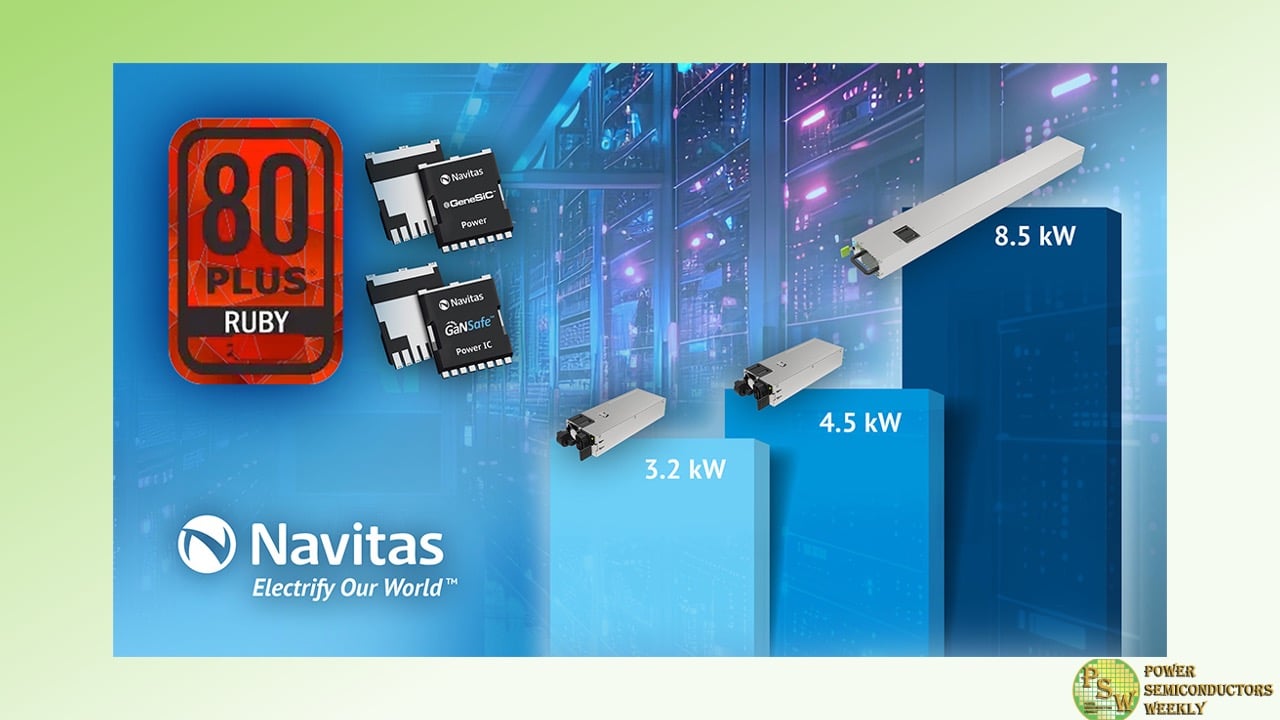
Navitas Semiconductor has announced that its portfolio of 3.2kW, 4.5kW, and 8.5 kW AI data center power supply unit (PSU) designs exceed the new 80 PLUS ‘Ruby’ certification, focused on the highest level of efficiency for redundant server data center PSUs.
The 80 PLUS certification program assesses and certifies the energy efficiency of internal PSUs in computers and servers. The ‘Ruby’ certification was announced in January 2025 by 80 PLUS’s administrating body, CLEAResult, following its endorsement by the Green Grid consortium.
‘Ruby’ is the most rigorous PSU efficiency standard since the ‘Titanium’ certification was released 14 years ago. In comparison, Ruby sets an additional 1% system efficiency across all load conditions, except at 50% load (which requires a 0.5% increase), to achieve a new benchmark of 96.5% efficiency.
This new standard offers the industry a clear path to enhanced energy efficiency, helping data centers address the evolving needs of cloud storage, commercial sectors, and the increasing pressure on the grid from AI computing. For example, every Ruby-certified 3.2 kW CRPS185 PSU can save up to 420 kilowatt-hours during a 3-year lifetime. That is the equivalent of over 400 kg of CO2 emissions.
Navitas exceeds both Ruby and Titanium certifications on their portfolio of AI data center PSU reference designs, ranging from 3.2 kW to 8.5 kW, and are powered by high-power GaNSafe™ ICs and GeneSiC™ Gen 3 ‘Fast’ SiC MOSFETs.
Navitas is the established leader in AI data center solutions enabled by GaN and SiC technology. In August 2023, they introduced a high-speed, high-efficiency 3.2 kW CRPS, achieving a 40% smaller size than best-in-class, legacy silicon solutions for power-hungry AI and Edge computing. This was followed by the world’s highest power density 4.5 kW CRPS, achieving a ground-breaking 137 W/in3, and efficiency of over 97%.
In November 2024, Navitas released the world’s first 8.5 kW AI data center power supply powered by GaN and SiC that could meet 98% efficiency, complying with the Open Compute Project (OCP) and Open Rack v3 (ORv3) specifications. Additionally, Navitas created IntelliWeave, an innovative patented new digital control technique, that when combined with high-power GaNSafe and Gen 3-Fast SiC MOSFETs, enables PFC peak efficiencies to 99.3% and reduces power losses by 30% reduction compared to existing solutions.
“Compared with Titanium, Ruby cuts the allowable PSU losses significantly and will be critical in enabling the data center industry to reduce its carbon footprint and cut operational costs,” said Gene Sheridan, CEO and co-founder of Navitas. “With the industry set to consume 1,000 TWh annually by next year1, every percentage point improvement in efficiency represents a reduction of 10 TWh, or approximately 3.5 million tons of CO22. Advances in our GaNFast and GeneSiC products enable these targets to be met and significantly exceeded.”
Navitas’ AI Power Roadmap and 80 PLUS Ruby-compliant demos can be viewed at the ‘Planet Navitas’ booth #1107 during the APEC 2025 conference, which takes place at Atlanta’s Georgia World Congress Center from March 16 to 20.
Original – Navitas Semiconductor
-

Navitas Semiconductor has announced a latest breakthrough of the world’s first production-released 650 V bi-directional GaNFast ICs and high-speed isolated gate-drivers, creating a paradigm shift in power with single-stage BDS converters, which enables the transition from two-stage to single-stage topologies. Targeted applications range widely and opens up multi-billion dollar market opportunities across EV charging (On-Board Chargers (OBC) and roadside), solar inverters, energy storage and motor drives. The recorded launch event video can be viewed here.
Over 70% of today’s high-voltage power converters use a ‘two-stage’ topology. For example, a typical AC-DC EV OBC implements an initial power-factor-correction (PFC) stage and a follow-on DC-DC stage, with bulky ‘DC-link’ buffering capacitors. The resulting systems are large, lossy, and expensive. Bi-directional GaNFast consolidates the two stages into a single, high-speed, high-efficiency stage and in the process, eliminates the bulky capacitors and input inductors – the ultimate solution in EV OBCs.
A leading EV and solar micro-inverter manufacturer have already begun their implementation of single-stage BDS converters to improve efficiency, size, and cost in their systems. GaNFast-enabled single-stage converters achieve up to 10% cost savings, 20% energy savings, and up to 50% size reductions.
The ultimate power semiconductor switch (transistor) can block voltage and allow current flow in two directions, with the highest efficiency. Navitas’ leadership in GaN innovation has delivered this landmark – the bi-directional GaNFast power IC.
Previously, two discrete, ‘back-to-back’ single switches had to be used, but new bi-directional GaNFast ICs are leading-edge, single-chip designs (monolithic integration) with a merged drain structure, two gate controls, and a patented, integrated, active substrate clamp. One high-speed, high-efficiency bi-directional GaNFast IC replaces up to 4 older switches, increasing system performance while reducing component count, PCB area, and system costs.
The initial 650 V bi-directional GaNFast ICs include NV6427 (100 mΩ RSS(ON) typ.) and NV6428 (50 mΩ RSS(ON) typ) in thermally enhanced, top-side-cooled TOLT-16L (Transistor Outline Leaded Topside-cooled) packaging. The product family will be extended into lower RSS(ON) offerings in the future.
The new, high-speed IsoFast devices are galvanically isolated, high-speed drivers optimized to drive bi-directional GaN. With 4x higher transient immunity than existing drivers (up to 200 V/ns) and no external negative bias supply needed, they deliver reliable, fast, accurate power control in high-voltage systems. Initial parts are the NV1702 (dual, independent-channel, digital, isolated bi-directional GaN gate driver) and NV1701 (half-bridge GaN digital isolator) in SOIC-16N and SOIC-14W packages.
“These ICs are a truly game-changing and disruptive technology both at the semiconductor and at the system level. They not only deliver improved efficiency, power density, simplicity, and system costs but will also transform multiple multi-billion-dollar markets in the most sustainable way possible.” Gene Sheridan, CEO and co-founder of Navitas commented. “The future of our electrified planet is bi-directional energy flow. From all renewable energy sources, the power grid, and all electrified applications, such as ESS, solar and EVs, energy should flow efficiently & bi-directionally, creating a critical new currency for our future planet. Single-stage BDS converters are the key for this inflection”.
Bi-directional GaNFast ICs (NV6427 and NV6428) are fully qualified and immediately available in mass-production quantities. IsoFast (NV1701 and NV1702) samples are available now to qualified customers.
Single-stage evaluation boards and user guide showcasing both IsoFast and bi-directional GaNFast ICs are available for qualified customers.
Navitas will feature bi-directional GaNFast ICs and IsoFast at the APEC 2025 power electronics conference in Atlanta, March 17th-19th, booth 1107.
Original – Navitas Semiconductor
-

Navitas Semiconductor announced unaudited financial results for the fourth quarter and full year ended December 31, 2024.
“I am proud of our team’s efforts to deliver growth in 2024, despite significant headwinds with an industry-wide slow-down in some major markets,” said Gene Sheridan, CEO and co-founder. “We achieved record GaN revenues from mobile, consumer and appliance sectors, while both GaN and SiC started shipping into data centers in the second half of 2024. We closed the year with an extraordinary $450 million of customer design-wins, which gives us increased confidence to resume a healthier growth rate in late ‘25 and beyond and continue to grow significantly faster than the overall power semiconductor market.”
4Q24 Financial Highlights
- Revenue: Total revenue was $18.0 million in the fourth quarter of 2024, compared to $26.1 million in the fourth quarter of 2023 and compared to $21.7 million in the third quarter of 2024.
- Loss from Operations: GAAP loss from operations for the quarter was $39.0 million, compared to a loss of $26.8 million for the fourth quarter of 2023 and a loss of $29.0 million for the third quarter of 2024. On a non-GAAP basis, loss from operations for the quarter was $12.7 million compared to a loss of $9.7 million for the fourth quarter of 2023 and a loss of $12.7 million in the third quarter of 2024.
- Cash: Cash and cash equivalents were $86.7 million as of December 31, 2024.
FY 2024 Financial Highlights
- Revenue: Total revenue grew to $83.3 million in 2024, a 5% increase from $79.5 million in 2023.
- Loss from Operations: GAAP loss from operations for the year was $130.7 million, compared to a loss of $118.1 million for 2023. On a non-GAAP basis, loss from operations for the year was $49.7 million compared to a loss of $40.3 million for 2023.
Market, Customer and Technology Highlights:
- Customer pipeline: increased 92% from $1.25 billion in December 2023, to $2.4 billion in December 2024.
- Data Center: AI driving fastest-growing end-market within customer pipeline, now valued at $165 million, up more than 100% vs. 2023; Navitas-designed 2.7 kW to 8.5 kW system platforms fueling 40 customer wins in 2024 with GaN and SiC AC-DC power supplies; now expanding into 48 V DC-DC converters with new 80-120 V GaN technology.
- EV: Over 40 customer wins in 2024 from US, Europe, Korea and China regions primarily with SiC in onboard and roadside chargers; first GaN EV win announced for 2026 production – extending driving range and reducing charging costs vs. traditional silicon on-board chargers.
- Mobile: Over 180 customer wins in 2024; continue to supply 10 of top 10 smartphone / notebook OEMs with Navitas GaN ICs; GaN reaches 10% adoption globally vs. silicon in mobile chargers and expands reach into Middle East, Africa, Latin America and India.
- Solar/Appliance/Industrial: On-track for GaN solar micro-inverter launch this summer expected to improve solar energy efficiencies, weight, size and cost; over 170 customer wins across solar, appliance and industrial.
Technology Announcement (March 12th live-stream event):
- Navitas will unveil a breakthrough in power conversion that will create a paradigm shift across multiple, major end markets. This includes both semiconductor and system-level innovations, and is expected to drive major improvements in energy efficiency and power density, further accelerating GaN and SiC adoption vs. legacy silicon devices. For more details, refer to: https://navitassemi.com/navitas-to-unveil-a-new-paradigm-in-power/.
Business Outlook
- First quarter 2025 net revenues are expected to be $13.0 to $15.0 million. Non-GAAP gross margin for the first quarter is expected to be 38% plus or minus 50 basis points, and non-GAAP operating expenses are expected to be approximately $18.0 million in the first quarter of 2025.
Original – Navitas Semiconductor
-

Navitas Semiconductor has announced it will attend APEC 2025 and highlight the latest advances in GaN and SiC wide bandgap technologies for AI data center EV, and mobile applications. Additionally, Navitas will highlight its latest ‘paradigm in power conversion’, unveiled in a live-streamed press event on the 12th of March.
APEC takes place at Atlanta’s Georgia World Congress Center from March 16th to 20th. The company’s “Planet Navitas” stand (Booth #1107) will showcase the company’s mission to ‘Electrify our World™’ by advancing the transition from legacy silicon to next-generation, clean energy GaN and SiC power semiconductors. These technologies are designed for high-growth markets that demand the highest efficiency and power density. The shift from silicon to GaN and SiC technologies has the potential to save over 6,000 megatons of CO2 per year by 2050. Recent Navitas breakthroughs that will be highlighted on the stand include:
- Navitas’ breakthrough that will create a paradigm shift in power conversion – full details will be unveiled in a live-streamed press event on the 12th of March.
- World’s First 8.5 kW AI Data Center Power Supply: See the world’s first 8.5 kW OCP power solution achieving 98% efficiency for AI and hyperscale data centers. Featuring high-power GaNSafe™ power ICs and Gen-3 Fast SiC MOSFETs in 3-Phase Interleaved CCM Totem-Pole PFC and 3-Phase LLC topologies to provide the highest efficiency, performance, and lowest component count.
- World’s Highest Power Density AI Power Supply: Navitas delivers efficient 4.5 kW power in the smallest power-supply form-factor for the latest AI GPUs that demand 3x more power per rack. The optimized design uses high-power GaNSafe ICs and Gen-3 Fast SiC MOSFETs enabling the world’s highest power density with 137 W/in3 and over 97% efficiency.
- ‘IntelliWeave’ Patented Digital Control Optimized for AI Data Center Power Supplies: Combined with high-power GaNSafe™ and Gen-3 ‘Fast’ SiC MOSFETs to enable PFC peak efficiencies of 99.3% and reduce power losses by 30% compared to existing solutions.
- Mid-voltage GaNFast FETs targeting 48V AI data center power supplies, next-generation EV platforms EV and AI-based robotics, to enable high-frequency, high-efficiency, and high-power density power conversion systems.
- GaNSlim™: Simple. Fast. Integrated: A new generation of highly integrated GaN power ICs that will further simplify and speed the development of small form factor, high-power-density applications by offering the highest level of integration and thermal performance. Target applications include chargers for mobile devices and laptops, TV power supplies, and lighting systems of up to 500W.
- Automotive Qualified (AEC-Q101) Gen-3 Fast SiC MOSFETs with ‘trench-assisted planar’ technology: Enabled by over 20 years of SiC innovation leadership, GeneSiC™ technology leads on performance with the Gen-3 ‘Fast’ SiC MOSFETs with ‘trench-assisted planar’ technology. This proprietary technology provides world-leading performance over temperature, delivering cool-running, fast-switching, and superior robustness to support faster charging EVs and up to 3x more powerful AI data centers.
- SiCPAK™ High-Power Modules – Built for Endurance and Performance: Utilizing industry-leading ‘trench-assisted planar’-gate technology and epoxy-resin potting for increased power cycling and long-lasting reliability, SiCPAK modules offer compact form factors and provide cost-effective, power-dense solutions for applications including EV charging, drives, solar, and energy storage systems (ESS).
- New Advancements in our Leading GaNFast & GeneSiC technology:
- GeneSiC MOSFETs specifically optimized for EV traction modules with additional screening and gold metallization for sintering.
- GaNSense™ motor drive ICs with bi-directional loss-less current sensing, voltage sensing, and temperature protection, further enhancing performance and robustness beyond what is achievable by any discrete GaN or discrete silicon device.
Navitas will participate and present in the Industry Session which showcases the latest work in all areas of power electronics.
Technical Presentations:
Wednesday 19th March
- ‘GaNSlim Power IC & DPAK-4L Package Enables 100W, 100cc, PD3.1 Continuous Power Solution with 95% Efficiency’
- 2:20 pm, IS14.3, A411, Tom Ribarich, Sr Dir. Strategic Marketing
- ‘500kHz Inverter Design Using Bidirectional GaN Switches’
- 8:30 am, IS11.1, A403, Jason Zhang, VP Applications & Technical Marketing
- ‘Advancing Power Solutions: Integrating Wide Bandgap Technologies for Next-Generation Applications’
- 1:30 pm – 4:55 pm ET, IS14, Llew Vaughan-Edmunds, Session Chair.
- ‘WBG Converter Design’
- 8:30 am – 11:55 am ET, IS11.1, Jason Zhang, Session Chair.
Thursday 20th March
- ‘Marketing & Technology Trends in Power Electronics’
- 10:10 AM – 11:50 AM ET, Stephen Oliver, Session Chair.
Original – Navitas Semiconductor
