-

Infineon Technologies AG provides its 600 V CoolMOS™ 8 high-voltage superjunction (SJ) MOSFET product family to LITEON, a leader in power management solutions, for superior efficiency and reliability in server applications. The 600 V CoolMOS 8 offers an all-in-one solution that improves LITEON’s new generation technology for existing and upcoming server application designs.
Infineon’s newest CoolMOS 8 at 600 V is leading the way in high-voltage superjunction MOSFET technology, setting the standard for both technology and price performance on a global scale. The technology increases the overall performance of systems, while also playing a crucial role in reducing carbon emissions in various applications, including chargers and adapters, solar and energy storage systems, EV charging infrastructure, and uninterruptible power supplies (UPS) for example.
The 600 V CoolMOS 8 SJ is designed to provide high efficiency and reliability, which aligns perfectly with LITEON’s and Infineon’s commitment to advancing performance and total-cost-of-ownership for server applications. Additionally, the .XT interconnect technology being a key feature of CoolMOS 8 makes the new generation a perfect fit for conventional and AI servers. The advanced interconnect technology offers industry leading thermal dissipation capabilities and improves electrical performance by reducing parasitic inductance and resistance. The CoolMOS 8 SJ MOSFETs have an 18 percent lower gate charge compared to previous MOSFET models and the quickest turn-off time in the market. Their thermal performance has been improved by 14 to 42 percent.
“Our CoolMOS 8 SJ MOSFETs achieve first-class power density and efficiency, which is essential for high-performance server applications,” said Richard Kuncic, Head of Power Systems at Infineon. “The all-in-one solution provided by the CoolMOS 8 product family simplifies our portfolio, making the selection process easier whilst reducing design-in efforts.”
“LITEON is excited to leverage Infineon’s CoolMOS 8 family in our next-generation server designs,” said John Chang, General Manager, Cloud Infrastructure Platform & Solution SBG, LITEON. “The superior efficiency and reliability of the 600 V CoolMOS 8 SJ underscores our commitment to delivering cutting-edge technology and energy-efficient solutions to our customers.”
The 600 V CoolMOS 8 SJ MOSFETs series is an “all in MOSFET” technology addressing industrial and consumer applications. Thanks to its integrated fast body diode, it enables usage of one MOSFET family across all main topologies in the targeted markets. It enables cost attractive Si-based solutions enhancing Infineon’s high-voltage wide band gap (WBG) offerings. The MOSFETs are available in SMD-QDPAK, TOLL and ThinTOLL-8×8 packages.
Samples of the 600 V CoolMOS 8 SJ MOSFETs are now available. More information is available at www.infineon.com/coolmos8. Learn more about the benefits of Infineon’s 600 V CoolMOS 8 SJ MOSFETs in the whitepaper here.
Original – Infineon Technologies
-

Infineon Technologies AG launched its new CoolSiC™ MOSFET 750 V G2 technology, designed to deliver improved system efficiency and increased power density in automotive and industrial power conversion applications. The CoolSiC MOSFETs 750 V G2 technology offers a granular portfolio with typical R DS(on) values up to 60 mΩ at 25°C, making it suitable for a wide range of applications, including on-board chargers (OBCs), DC-DC converters, auxiliaries for electric vehicles (xEVs) as well as industrial applications in EV charging, solar inverter, energy storage systems, telecom and SMPS.
The ultra-low R DS(on) values 4 and 7 mΩ enable outstanding performance in static-switching applications, making the MOSFETs a perfect choice for applications such as eFuse, high-voltage battery disconnect switches, solid-state circuit breakers, and solid-state relays. The best-in-class lowest R DS(on) 4 mΩ is featured in Infineon’s innovative top-side cooled Q-DPAK package, which is designed to provide optimal thermal performance and reliability.
The technology also exhibits excellent R DS(on) x Q OSS and best-in-class R DS(on) x Q fr, contributing to reduced switching loss in both hard-switching and soft-switching topologies with superior efficiency in hard-switching user cases. With reduced gate charge, the technology allows for faster switching and reduces gate drive losses, making them more efficient in high-frequency applications.
Additionally, the CoolSiC MOSFETs 750 V G2 offer a combination of high threshold voltage V GS(th),typ of 4.5 V at 25°C and ultra-low Q GD/Q GS ratio, which reinforce robustness against parasitic turn-on (PTO). Furthermore, the technology allows for extended gate driving capabilities, supporting static gate voltages of up to -7 V and transient gate voltages of up to -11 V. This enhanced voltage tolerance provides engineers with greater design margins and best compatibility with other devices in the market.
The CoolSiC 750 V G2 delivers unparalleled switching performance, great ease-of-use and superior reliability with firm adherence to AEC Q101 standards for automotive-grade parts and JEDEC standard for industrial-grade parts. It enables a more efficient, compact and cost-effective designs to fulfill the ever‑growing market needs and underscores its commitment to reliability and longevity in safety-critical automotive applications.
Infineon’s CoolSiC MOSFET 750 V G2 Q-DPAK 4/7/16/25/60 mΩ samples are available to order. More information is available at www.infineon.com/coolsic-750v
Original – Infineon Technologies
-

In a major step toward advancing renewable energy technologies, SMA Solar Technology AG has selected a new high-performance power module from Semikron Danfoss, integrating ROHM’s latest 2kV Silicon Carbide (SiC) MOSFETs. This collaboration marks a milestone in the evolution of high-voltage solar inverter solutions.
The new SEMITOP E1/E2 SiC power module from Semikron Danfoss combines compact design with cutting-edge 2kV-rated SiC MOSFETs from ROHM. Tailored specifically for solar applications, the solution addresses the rising demands for higher voltage, increased efficiency, and greater system reliability.
Key Benefits:
- Higher System Voltage: Enables 1500V DC systems with reduced derating margins, maximizing energy yield.
- Improved Efficiency: SiC technology dramatically reduces switching losses compared to traditional silicon, enhancing overall inverter performance.
- Compact Design: Supports smaller inverter footprints and lower system costs due to reduced cooling requirements and simpler circuitry.
- Extended Lifetime: Enhanced reliability and ruggedness, crucial for long-term solar energy deployments.
By adopting Semikron Danfoss’ advanced SiC modules, SMA positions itself at the forefront of the solar inverter industry, delivering more efficient and resilient solutions for the fast-growing global renewable energy market.
This partnership underlines the growing importance of wide-bandgap semiconductors like SiC in renewable energy applications. As the demand for high-efficiency, high-voltage solar inverters continues to soar, collaborations like this set new industry benchmarks for performance and sustainability.
Original – Semikron Danfoss
-

ROHM has developed the new 4-in-1 and 6-in-1 SiC molded modules in the HSDIP20 package optimized for PFC and LLC converters in onboard chargers (OBC) for xEVs (electric vehicles). The lineup includes six models rated at 750V (BSTxxx1P4K01) and seven products rated at 1200V (BSTxxx2P4K01). All basic circuits required for power conversion in various high-power applications are integrated into a compact module package, reducing the design workload for manufacturers and enabling the miniaturization of power conversion circuits in OBCs and other applications.
In recent years, the rapid electrification of cars is driving efforts to achieve a decarbonized society. Electric vehicles are seeing higher battery voltages to extend the cruising range and improve charging speed, creating a demand for higher output from OBCs and DC-DC converters. At the same time, there is an increasing need in the market for greater miniaturization and lighter weight for these applications, requiring technological breakthroughs to improve power density – a key factor – while enhancing heat dissipation characteristics that could otherwise hinder progress.
ROHM’s HSDIP20 package addresses these technical challenges that were previously becoming difficult to overcome with discrete configurations, contributing to both higher output and the downsizing of electric powertrains.
The HSDIP20 features an insulating substrate with excellent heat dissipation properties that suppresses the chip temperature rise even during high power operation. When comparing a typical OBC PFC circuit utilizing six discrete SiC MOSFETs with top-side heat dissipation to ROHM’s 6-in-1 module under the same conditions, the HSDIP20 package was verified to be approx. 38°C cooler (at 25W operation).
This high heat dissipation performance supports high currents even in a compact package, achieving industry-leading power density more than three times higher than top-side cooled discretes and over 1.4 times that of similar DIP type modules. As a result, in the PFC circuit mentioned above, the HSDIP20 can reduce mounting area by approx. 52% compared to top-side cooled discrete configurations, greatly contributing to the miniaturization of power conversion circuits in applications such as OBCs.
Going forward, ROHM will continue to advance the development of SiC modules that balance miniaturization with high efficiency while also focusing on the development of automotive SiC IPMs that provide higher reliability in a smaller form factor.
Original – ROHM
-

SemiQ Inc has announced a family of co-packaged 1200 V SOT-227 MOSFET modules based on its third-generation SiC technology.
In addition to smaller die sizes, third generation SIC devices offer faster switching speeds and reduced losses.
The family of highly rugged and easy mount devices currently offers six devices with an RDSon range of 8.4 to 39 mΩ: GCMS008C120S1-E1, GCMX008C120S1-E1, GCMS016C120S1-E1, GCMX016C120S1-E1, GCMS040C120S1-E1 and GCMX040C120S1-E1, with the GCMX040C120S1-E1 having a switching time as low as 67 ns. In addition to these six, two further modules – GCMS080C120S1-E1 and GCMX080C120S1-E1 – are available, each with an RDSon of 80 mΩ.
The COPACK MOSFETs with Schottky barrier diode provides exceptional switching losses at high junction temperature due to the low turn on switching losses.
SemiQ is targeting the robust SiC MOSFET modules at applications including solar inverters, energy storage systems, battery charging, and server power supplies. All devices have been screened with wafer-level gate-oxide burn-in tests and tested beyond 1400 V, with avalanche testing to 330 mJ (RDSon = 39 mΩ) or 800 mJ (RDSon = 16.5 or 8.4 mΩ).
In addition to having a drain-to-source voltage (VDS) of 1200 V, the MOSFET reduces total switching losses to as low as 468 µJ and a reverse recovery charge of 172 nC (GCMX040C120S1-E1). The family also has a low junction-to-case thermal resistance and comes with an isolated backplate and the ability to directly mount to a heatsink by 4kVAC galvanic isolation testing.
Specifications: Ratings and electrical/thermal characteristics
The QSiC 1200 V MOSFET modules have a continuous operational and storage temperature of -55oC to 175oC. It has a recommended operational gate-source voltage of -4.5/18 V, with a VGSmax of -8/22 V, and a power dissipation of 183 to 536 W (RDSon = 39 and mΩ, core and junction temperature 25oC).
For static electrical characteristics, the device has a junction-to-case thermal resistance of 0.23oC per watt (RDSon = 8.4) as well as a typical zero-gate voltage drain current of 100 nA, and a gate-source voltage current of 10 nA.
The fastest switching device has a turn-on delay time of 13 ns with a rise time of 7 ns; its turn-off delay time is 18 ns with a fall time of 29 ns.
Original – SemiQ
-
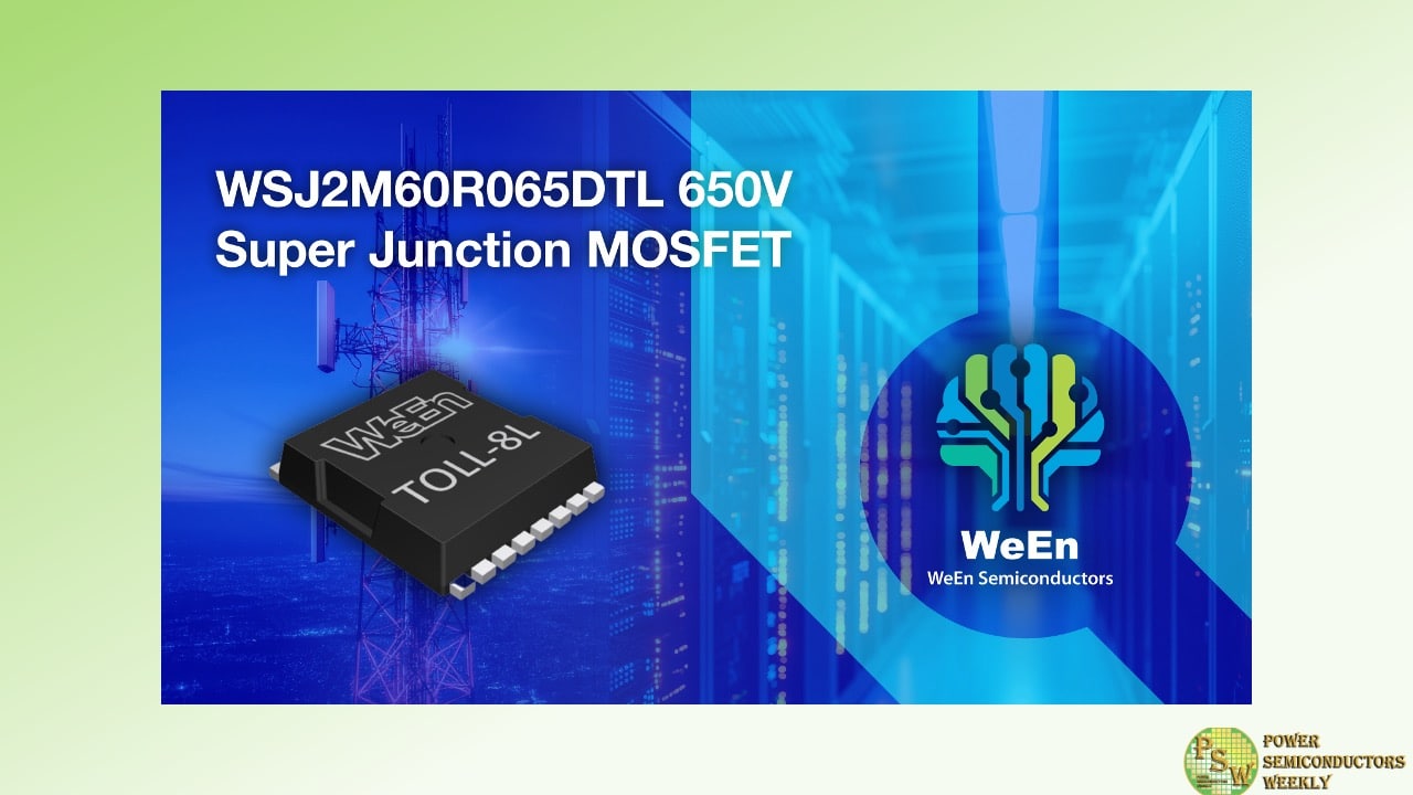
WeEn Semiconductors will exhibit the company’s latest 600 V super junction MOSFET for computing and telecoms server applications at this year’s PCIM Expo conference and trade fair. The WSJ2M60R065DTL has been specifically developed to address the demands of artificial intelligence (AI) and other high-performance processing applications by enabling improved efficiency, smaller form factors and easier thermal management.
Based on the company’s latest generation super junction technology, the WeEn WSJ2M60R065DTL super junction MOSFET combines an industry-leading on resistance (RDS(ON)) and figure of merit (RDS(ON)*Qg) with an ultra-compact TOLL package. Visitors to PCIM in Nuremberg from 6th – 8th May 2025 will have the opportunity to see this advanced technology on the WeEn booth (Hall 9, booth 131), alongside other bipolar products including silicon-controlled rectifiers, power diodes, high voltage transistors and silicon carbide (SiC) devices.
The WSJ2M60R065DTL is rated for 50 A, features a maximum RDS(ON) of 65 mΩ and has a typical blocking voltage of around 700 V. An integrated and fine-tuned forward recovery diode (FRD) ensures excellent reverse recovery robustness and balanced high-temperature performance. The body diode can withstand a commutation speed of 1000 A/μs without damage, making the WSJ2M60R065DTL particularly suitable for Zero Voltage Switching (ZVS) applications in soft-switching topologies where it can deliver high efficiency while handling irregular operating conditions. At the same time, stable resistance performance delivers a steady and predictable RDS(ON) across a range of current and temperature conditions.
In developing the new MOSFET, WeEn has focused on precise control of the charge balance of the super junction structure. This ensures robust avalanche ruggedness and low capacitive losses that allow for an optimized balance of RDS(ON) and EOSS As with all WeEn technologies, reliability is a prime consideration and the company conducts extensive and reliability checks. All of the company’s super junction MOSFETs demonstrate not only consistency among samples but good ESD capabilities and zero aging during reliability examinations.
Original – WeEn Semiconductors
-

Navitas Semiconductor announced the release of its latest SiCPAK™ power modules with epoxy-resin potting technology, powered by proprietary trench-assisted planar SiC MOSFET technology, that have been rigorously designed and validated for the most demanding high-power environments, prioritizing reliability and high-temperature performance. Target markets include EV DC fast chargers (DCFC), industrial motor drives, interruptible power supplies (UPS), solar inverters and power optimizers, energy storage systems (ESS), industrial welding, and induction heating.
The new portfolio of 1200V SiCPAK™ power modules, enabled by advanced epoxy-resin potting technology, are engineered to withstand high-humidity environments by preventing moisture ingression and enable stable thermal performance by reducing degradation from power and temperature variations.
Navitas’ SiCPAK™ modules demonstrated 5x lower thermal resistance increase following 1000 cycles of thermal shock testing (-40 C to + 125 C) compared to conventional silicone-gel-filled case-type modules. Furthermore, all silicone-gel-filled modules failed isolation tests while SiCPAK™ epoxy-resin potted modules maintained acceptable isolation levels.
Enabled by over 20 years of SiC innovation leadership, Navitas’ GeneSiC™ ‘trench-assisted planar SiC MOSFET technology’ provides industry-leading performance over temperature, enabling up to 20% lower losses, cooler operation, and superior robustness to support long-term system reliability.
The ‘trench-assisted planar’ technology enables an extremely low RDS(ON) increase versus temperature, which results in the lowest power losses across a wider operating range and offers up to 20% lower RDS(ON) under in-circuit operation at high temperatures compared to competition. Additionally, all GeneSiC™ SiC MOSFETs have the highest-published 100%-tested avalanche capability, up to 30% better short-circuit withstand energy, and tight threshold voltage distributions for easy paralleling.
The 1200V SiCPAK™ power modules have built-in NTC thermistors and are available from 4.6 mΩ to 18.5 mΩ ratings in half-bridge, full-bridge, and 3L-T-NPC circuit configurations. They are pin-to-pin compatible with industry-standard press-fit modules. Additionally, optional pre-applied Thermal Interface Material (TIM) for simplified assembly is available.
Original – Navitas Semiconductor
-

Mitsubishi Electric Corporation announced that it will begin shipping samples of two new SLIMDIP series power semiconductor modules for room air conditioners and other home appliances, the Full SiC (silicon carbide) SLIMDIP (PSF15SG1G6) and the Hybrid SiC SLIMDIP (PSH15SG1G6), on April 22.
Both modules, the first SiC versions in the company’s SLIMDIP series of compact, terminal-optimized modules, achieve excellent output and power loss reduction for energy savings in small- to large-capacity appliances. They will be exhibited at Power Conversion Intelligent Motion (PCIM) Expo & Conference 2025 in Nuremberg, Germany from May 6 to 8, as well as trade shows in Japan, China and other countries.
Mitsubishi Electric’s newly developed silicon carbide metal-oxide-semiconductor field-effect transistor (SiC-MOSFET) chip is incorporated into both new SLIMDIP packages. Compared to current silicon (Si)-based reverse-conducting insulated-gate bipolar transistor (RC-IGBT) SLIMDIP modules, these new SiC modules achieve higher output for larger-capacity appliances. Additionally, compared to the Si-based module, power loss is reduced by 79% with the Full SiC SLIMDIP and by 47% with the Hybrid SiC SLIMDIP for more energy-efficient appliances.
With these two new modules as well as existing Si-based RC-IGBT SLIMDIP modules, the SLIMDIP series now offers three options for use in inverter boards of appliances such as room air conditioners, each one suited to specific electrical capacity and performance needs, but all offered in the same package to help reduce the burden of designing inverter substrates.
Original – Mitsubishi Electric
-

ROHM has developed N-channel power MOSFETs featuring industry-leading low ON-resistance and wide SOA capability. They are designed for power supplies inside high-performance enterprise and AI servers.
The advancement of high-level data processing technologies and the acceleration of digital transformation have increased the demand for data center servers. At the same time, the number of servers equipped with advanced computing capabilities for AI processing is on the rise and is expected to continue to grow. These servers operate 24 hours a day, 7 days a week – ensuring continuous operation. As a result, conduction losses caused by the ON-resistance of multiple MOSFETs in the power block have a significant impact on system performance and energy efficiency. This becomes particularly evident in AC-DC conversion circuits, where conduction losses make up a substantial portion of total power loss – driving the need for low ON-resistance MOSFETs.
Additionally, servers equipped with a standard hot-swap function, which allow for the replacement and maintenance of internal boards and storage devices while powered ON, experience a high inrush current during component exchanges. Therefore, to protect server components and MOSFETs from damage, a wide Safe Operating Area (SOA) tolerance is essential.
To address these challenges, ROHM has developed its new DFN5060-8S package that supports the packaging of a larger die compared to conventional designs, resulting in a lineup of power MOSFETs that achieve industry-leading low ON-resistance along with wide SOA capability. These new products significantly contribute to improving efficiency and enhancing reliability in server power circuits.
The new lineup includes three products. The RS7E200BG (30V) is optimized for both secondary-side AC-DC conversion circuits and hot-swap controller (HSC) circuits in 12V power supplies used in high-performance enterprise servers. The RS7N200BH (80V) and RS7N160BH (80V) are ideal for secondary AC-DC conversion circuits in 48V AI server power supplies.
All three models feature the newly developed DFN5060-8S package (5.0mm × 6.0mm). The package increases the internal die size area by approximately 65% compared to the conventional HSOP8 package (5.0mm × 6.0mm). As a result, the RS7E200BG (30V) and RS7N200BH (80V) achieve ON-resistances of 0.53mΩ and 1.7mΩ (at VGS = 10V), respectively – both of which rank among the best in the industry in the 5.0mm × 6.0mm class, significantly contributing to higher efficiency in server power circuits.
Moreover, ROHM has optimized the internal clip design to enhance heat dissipation, further improving SOA tolerance, which contributes to ensuring application reliability. Notably, the RS7E200BG (30V) achieves an SOA tolerance of over 70A at a pulse width of 1ms and VDS = 12V, which is twice that of the conventional HSOP8 package MOSFETs under the same conditions, ensuring industry-leading SOA performance in a 5.0mm × 6.0mm footprint.
Going forward, ROHM plans to gradually begin mass production of power MOSFETs compatible with hot-swap controller circuits for AI servers in 2025, continuing to expand its lineup that contributes to greater efficiency and reliability across a wide range of applications.
Original – ROHM
-

Vishay Intertechnology, Inc. introduced a new Gen 4.5 650 V E Series power MOSFET that delivers high efficiency and power density for telecom, industrial, and computing applications. Compared to previous-generation devices, the Vishay Siliconix n-channel SiHK050N65E slashes on-resistance by 48.2 %, while offering a 65.4 % lower resistance times gate charge, a key figure of merit (FOM) for 650 V MOSFETs used in power conversion applications.
Vishay offers a broad line of MOSFET technologies that support all stages of the power conversion process, from high voltage inputs to the low voltage outputs required to power the latest high tech equipment. With the SiHK050N65E and other devices in the Gen 4.5 650 V E Series family, the company is addressing the need for efficiency and power density improvements in two of the first stages of the power system architecture — power factor correction (PFC) and subsequent DC/DC converter blocks.
Typical applications will include servers, edge computing, and super computers; UPS; high intensity discharge (HID) lamps and fluorescent ballast lighting; telecom SMPS; solar inverters; welding equipment; induction heating; motor drives; and battery chargers.
Built on Vishay’s latest energy-efficient E Series superjunction technology, the SiHK050N65E’s low typical on-resistance of 0.048 Ω at 10 V results in a higher power rating for applications > 6 kW. With 50 V of additional breakdown voltage, the 650 V device addresses 200 VAC to 277 VAC input voltages and the Open Compute Project’s Open Rack V3 (ORV3) standards. In addition, the MOSFET offers ultra low gate charge down to 78 nC. The resulting FOM of 3.74 Ω*nC translates into reduced conduction and switching losses to save energy and increase efficiency. This allows the device to address the specific titanium efficiency requirements in server power supplies or reach 96 % peak efficiency.
For improved switching performance in hard-switched topologies such as PFC and two-switch forward designs, the MOSFET released today provides low typical effective output capacitances Co(er) and Co(tr) of 167 pF and 1119 pF, respectively. The device’s resulting resistance times Co(er) FOM is an industry-low 8.0 Ω*pF. The SiHK050N65E is offered in the PowerPAK® 10 x 12 package with a Kelvin connection for reduced gate noise and provides increased dv/dt ruggedness. RoHS-compliant and halogen-free, the MOSFET is designed to withstand overvoltage transients in avalanche mode with guaranteed limits through 100 % UIS testing.
Original – Vishay Intertechnology
