-

Infineon Technologies AG expanded the lawsuit pending before the District Court for the Northern District of California on 23 July 2024, adding claims against Innoscience (Zhuhai) Technology Company, Ltd., and Innoscience America, Inc. and affiliates based on the infringement of three additional patents referring to gallium nitride (GaN) technology owned by Infineon. In addition, Infineon today filed a complaint with the U.S. International Trade Commission (USITC) containing legal claims referring to the same four patents covered by the lawsuit.
Infineon seeks a permanent injunction for the infringement of United States patents referring to gallium nitride (GaN) technology owned by Infineon. The patent claims cover core aspects of GaN power semiconductors encompassing innovations that enable performance and reliability of Infineon’s proprietary GaN power transistors.
Already, on 14 March 2024, Infineon filed a patent infringement suit against Innoscience in the United States with the District Court for the Northern District of California. On 4 June 2024, Infineon filed a corresponding lawsuit with the District Court Munich, Germany. Additional lawsuits were filed against distributors of Innoscience in Germany.
Furthermore, Infineon successfully filed for a preliminary injunction (court order), which the District Court Munich issued on 12 June 2024. According to this court order Innoscience was obligated to remove all infringing product from their booth at the international power electronics trade show PCIM Europe.
Infineon leads the industry with its GaN patent portfolio, comprising approximately 350 patent families. Infineon’s portfolio of silicon, silicon carbide, gallium nitride power transistors and complementary drivers and controllers was enhanced with the October 2023 acquisition of GaN Systems Inc. The acquisition boosted Infineon’s GaN offering and further expanded its leading position in power semiconductors.
Original – Infineon Technologies
-

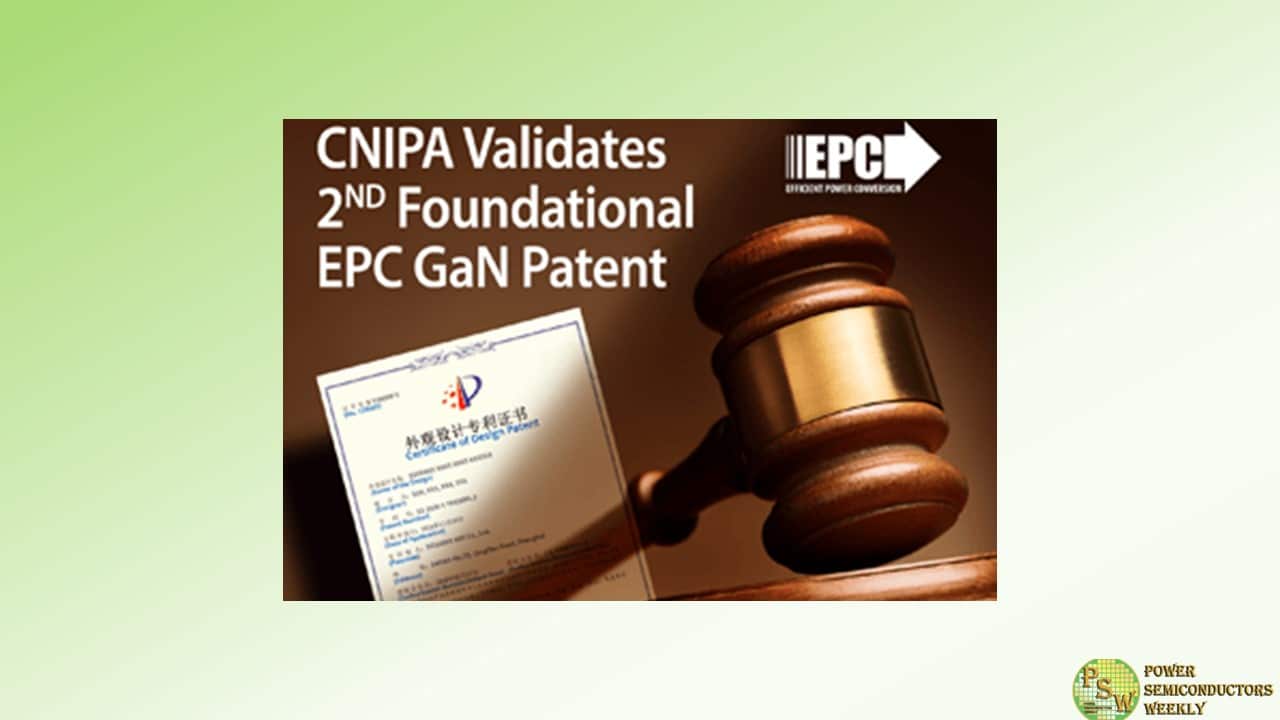
Efficient Power Conversion (EPC) announced that it has moved one step closer to achieving preeminence in the gallium nitride (GaN) power semiconductor industry, as its intellectual property rights to this revolutionary technology were upheld for the third time in three months. The next-generation wide bandgap semiconductors developed by EPC are essential to artificial intelligence (AI), satellites, fast chargers, lidar, humanoid robots and many other transformational technologies.
The U.S. International Trade Commission (ITC) found two of EPC’s key patents valid and one, the Company’s foundational patent, infringed by Innoscience (Zhuhai) Technology Co., Ltd. and its affiliate, Innoscience America, Inc. The ITC’s recommendation comes on the heels of two recent decisions from the China National Intellectual Property Administration (CNIPA), which similarly validated EPC’s counterpart patents in China. The ITC initial determination is a significant milestone in solidifying EPC’s leadership in wide bandgap semiconductors and could lead to a ban later this year on importation of Innoscience’s infringing products into the United States.
“The ITC’s finding that Innoscience uses our patented technology without authorization puts EPC in an enviable position, as U.S. and Chinese regulatory bodies have upheld the validity of our patents,” said Alex Lidow, CEO and Co-Founder of EPC.
“The Commission’s recommendations validate nearly two decades of hard work, resources and R&D that went into developing EPC’s uniquely valuable intellectual property portfolio,” Dr. Lidow added.
Over the last 15 years, EPC has capitalized on its first-mover advantage to develop a broad portfolio of over 200 GaN-related patents and over 150 products, which include its rapidly growing family of integrated circuits, automotive qualified and radiation hardened devices.
Compared with traditional silicon-based power devices, GaN represents a significant leap, with higher efficiency, faster switching speeds, smaller size and lower cost. GaN power devices are integral to self-driving vehicles, medical and communications devices, next-generation rapid chargers, drones, satellites, data centers, e-bikes, solar power systems and humanoid robots, among many other applications. Most notably, EPC’s cutting-edge semiconductors are central to powering the AI revolution by significantly freeing up space for extra computing power while simultaneously reducing energy consumption.
The ITC’s preliminary ruling found both U.S. patents that EPC asserted against Innoscience valid. It also found “infringement [by Innoscience] of U.S. Patent No. 8,350,294,” EPC’s foundational patent used broadly across multiple industries. The second EPC patent, U.S. Patent No. 8,404,508, was found valid, but not infringed by Innoscience. The Commission’s final determination is expected to be issued on November 5, 2024.
Original – Efficient Power Conversion
-
Efficient Power Conversion Corp (“EPC”) announced that the China National Intellectual Property Administration (“CNIPA”) has validated the claims of EPC patent titled “Compensated gate MISFET and method for fabricating the same” (Chinese Patent No. ZL201080015425.X) for enhancement-mode GaN semiconductor devices.
The decision on April 30, 2024 follows an April 2, 2024 announcement from the CNIPA that confirmed the validity of key claims of EPC’s Chinese patent titled “Enhancement mode GaN HEMT device and method for fabricating the same” (Chinese Patent No. ZL201080015388.2). Both EPC patents were challenged by Innoscience (Suzhou) Technology Co., Ltd. (“Innoscience”).
Compared with traditional silicon-based power devices, GaN technology represents a transformational leap with higher efficiency, faster switching speeds and smaller size. GaN devices are used in artificial intelligence servers, self-driving vehicles, next-generation rapid chargers, drones, e-bikes, and humanoid robots, among other applications. Chinese Patent No. ZL201080015425.X covers the fundamental design and configuration of EPC’s proprietary enhancement mode GaN field effect transistors (FETs) with reduced gate leakage. Most industry participants employ the GaN gate technology covered by this patent.
“These are two of the foundational patents supporting our broad portfolio of innovations, and we are pleased that the CNIPA has again confirmed the validity of our valuable intellectual property,” said Alex Lidow, CEO and Co-founder of EPC. “Quick, fair and efficient decisions such as these reinforce the confidence in legal systems that companies need to operate globally.”
In May 2023, EPC filed complaints in the U.S. federal court in Los Angeles and in the U.S. International Trade Commission, asserting that Innoscience (Zhuhai) Technology Co., Ltd. and its affiliates infringe patents of its foundational patent portfolio, which include the U.S. counterparts of EPC’s Chinese Patent Nos. ZL201080015425.X and ZL201080015388.2. In response, Innoscience had petitioned the CNIPA to invalidate the two Chinese patents.
Original – Efficient Power Conversion
-

Innoscience Technology welcomes, with thanks, two additional decisions, from March 26, 2024, by the United States Patent and Trademark Office (USPTO) to institute review of the validity of yet another two (and still additional) U.S. patents of Efficient Power Conversion Corporation (“EPC”).
The two additional U.S. patents, which are now under review at the USPTO, were previously asserted by EPC at the beginning of the legal dispute initiated by EPC in the U.S. International Trade Commission (ITC). During the course of that proceeding, however, EPC withdrew these patents, but Innoscience maintained its challenges of these patents at the USPTO.
In the March 26, 2024 decisions, the USPTO decided to institute the review of the validity of these two further U.S. patents, as previously asserted by EPC in the ITC proceeding. These new decisions to institute now supplement two other and prior decisions to institute by the USPTO, relating to the other two patents that are still asserted by EPC at the ITC.
Now, in all four decisions, the USPTO has concluded that “there is a reasonable likelihood that Petitioner [Innoscience] would prevail with respect to at least one of the claims challenged in the Petition.” Innoscience has achieved, via the preliminary decisions, a perfect 4-for-4 record at the USPTO.
Also, now all patents that were asserted by EPC now are under review by the USPTO. These new March 26, 2024 rulings by the USPTO are only the latest developments related to EPC’s misguided lawsuits against Innoscience, wherein EPC continues to struggle in its meritless attacks on Innoscience. In all four rulings now, including from March 20 and March 26, 2024, three judges from the USPTO have initially agreed with Innoscience, that the EPC patents that Innoscience challenged at the USPTO are invalid.
And, once again, in this new set, Innoscience again argued to the USPTO that the challenged EPC patent was invalid, based on a prior patent of an EPC cofounder/inventor when he was at International Rectifier, and on a preliminary basis, according to the institution decision, the USPTO agreed with Innoscience. In all four proceedings, Innoscience has described multiple reasons why the four EPC patents are invalid, and for virtually every argument on invalidity, the USPTO initially agreed. Next, the USPTO will receive additional briefing and make final determinations by March 26, 2025.
Innoscience is confident that it will achieve an eventual complete victory in the dispute with EPC. With these recent USPTO decisions of March 26, 2024, Innoscience continues to achieve successes in its legal dispute with EPC, and the additional USPTO decisions repeatedly demonstrate that EPC’s accusations against Innoscience lack merit, given that the USPTO has now determined, at least initially, that all four EPC patents asserted by EPC are likely invalid.
Original – Innoscience Technology
-

According to the information on the official website of the China National Intellectual Property Administration (CNIPA) on April 2, 2024, the key claims 6, 9, 10, 13, 14, 17, 18 and 22-26 of the Chinese patent titled “Enhancement mode GaN HEMT device and method for fabricating the same” (Patent No. ZL201080015388.2) owned by Efficient Power Conversion Corp (“EPC”) have been maintained valid during an invalidation procedure (case number: 4W116775), which was requested by the petitioner Innoscience (Suzhou) Technology Co., Ltd. (“Innoscience”).
As compared with products using silicon-based devices, transistors and integrated circuits using GaN-based technology are superior in terms of higher efficiency, reduced weight and lower cost. The key claims which are held valid as mentioned above cover core technologies of the design and the manufacturing process of EPC’s proprietary enhancement-mode GaN-based power semiconductor devices. By virtue of multiple innovations including such technologies, EPC has successfully brought GaN-based power devices from laboratory to market.
In May 2023, EPC filed complaints before the US Federal Court and the US International Trade Commission (ITC), asserting that Innoscience (Zhuhai) Technology Co., Ltd. and its affiliate Innoscience infringed four patents of its foundational patent portfolio, which include the US counterpart of this Chinese patent ZL201080015388.2. As part of the responses to those complaints, Innoscience filed, in September 2023, a request to invalidate the EPC’s Chinese counterpart patent ZL201080015388.2 before the CNIPA.
Pursuant to the Chinese Patent Law, Innoscience may appeal this invalidation decision before the Beijing Intellectual Property Court within three months.
Original – Efficient Power Conversion
-

Innoscience Technology firmly denounces the accusations made by Infineon Technologies Austria AG in a recent patent infringement lawsuit against three Innoscience entities. Infineon filed this lawsuit in a U.S. district court in California on March 13, 2024, and asserted a single U.S. patent.
Innoscience denies Infineon’s allegations of patent infringement as well as the validity of the Infineon patent. Innoscience will vigorously defend itself and is confident that it will prevail. Infineon’s intention with this litigation is also in question, as it has asserted a patent that has significant defects. Particularly, even a cursory review of Infineon’s patent portfolio reveals that the alleged “invention” of the asserted patent was already disclosed in Infineon’s own earlier prior art patents, raising concerns that it may have committed fraud on the United States Patent and Trademark Office, for not making proper disclosures during the prosecution of the asserted defective patent.
In addition, contrary to Infineon’s wrong characterization that the claims of the asserted defective patent “cover core aspects of GaN power semiconductors,” the lawsuit only concerns a small fraction of Innoscience’s packaged high-voltage (650V-700V) GaN transistors and does not affect the vast majority of its other products (including unpackaged transistors and wafers, low-voltage transistors, and certain packaged transistors).
Therefore, the lawsuit should have little to no effect on Innoscience’s current ability to make, use, sell, offer to sell, or import into the United States its products for customers. Innoscience respects others’ valid IP rights and is also dedicated to developing its own IP portfolio. Despite being an eight-year old company, Innoscience has filed more than 800 patent applications globally. Innoscience’s R&D team boasts 500+ technical experts across the world.
Through continuing innovation, Innoscience has produced GaN devices to power a diverse range of products, from power delivery chargers to data centers and smartphones, showcasing its ability to align with evolving application demands and adapt to diverse customer specifications.
Moreover, Innoscience has always sought a cooperative and mutually beneficial approach to develop the global GaN industry, even among others in the same industry. Innoscience intends to prevail in this pending lawsuit and is determined to remain a trusted and reliable partner for its customers and contribute to their success by offering top-notch and versatile products and solutions based on Innoscience’s home-grown, superior technologies.
Original – Innoscience Technology
-

Infineon Technologies AG filed a lawsuit, through its subsidiary Infineon Technologies Austria AG, against Innoscience (Zhuhai) Technology Company, Ltd., and Innoscience America, Inc. and affiliates. Infineon is seeking permanent injunction for infringement of a United States patent relating to gallium nitride (GaN) technology owned by Infineon.
The patent claims cover core aspects of GaN power semiconductors encompassing innovations that enable the reliability and performance of Infineon’s proprietary GaN devices. The lawsuit was filed in the district court of the Northern District of California.
Infineon alleges that Innoscience infringes the Infineon patent mentioned above by making, using, selling, offering to sell and/or importing into the United States various products, including GaN transistors for numerous applications, within automotive, data centers, solar, motor drives, consumer electronics, and related products used in automotive, industrial, and commercial applications.
“The production of gallium nitride power transistors requires completely new semiconductor designs and processes”, said Adam White, President of Infineon’s Power & Sensor Systems Division. “With nearly two decades of GaN experience, Infineon can guarantee the outstanding quality required for the highest performance in the respective end products. We vigorously protect our intellectual property and thus act in the interest of all customers and end users.”
Infineon has been investing in R&D, product development and the manufacturing expertise related to GaN technology for decades. Infineon continues to defend its intellectual property and protect its investments.
On 24 October 2023, Infineon announced the closing of the acquisition of GaN Systems Inc., becoming a leading GaN power house and further expanding its leading position in power semiconductors.
Infineon leads the industry with its GaN patent portfolio, comprising around 350 patent families. Market analysts expect the GaN revenue for power applications to grow by 49% CAGR to approx. US$2 billion by 2028 (source: Yole, Power SiC and GaN Compound Semiconductor Market Monitor Q4 2023). Gallium nitride is a wide bandgap semiconductor with superior switching performance that allows smaller size, higher efficiency and lower-cost power systems.
Original – Infineon Technologies
-

Innoscience Technology will demonstrate industry-leadership at the upcoming IEEE Applied Power Electronics Conference and Exposition (APEC) 2024.
At the industrial session, Innoscience will address the exponential demand in power by datacenters due to the processing power necessitated by Artificial Intelligence (AI) applications. The paper will show that with Innoscience’s 650V InnoGaN, it is possible to make a 2kW AC/DC conversion PSU with a high power density and a peak efficiency above 96%, thereby meeting the recent stringent 80 Plus titanium efficiency rating.
Thanks to the absence of a body diode on GaN devices, a simple Totem pole PFC architecture can be implemented while still reaching high levels of efficiency. At the booth Innoscience will also showcase a 4.2kW AC/DC conversion PSU meeting 80 Plus titanium efficiency rating within a power density of 130W/in3.
Moreover, to address the 48V to 12V DC-DC power conversion inside the data center, Innoscience will present an all GaN HEMTs based 1kW 48V-12V unregulated LLC solution that features GaN power devices both at the primary side (100V devices) as well as at the secondary side (40V devices). In order to maximize the power density and simplify the circuit, the solution uses Innoscience’s recent integrated SolidGaN solution (ISG3201), which integrates an half-bridge (made by two 100V/3.2mOhm InnoGaN devices) with its driver, protection etc.. in one package. The final all GaN 1kW 48V-12 converter has a size of only 50mmx30mmx9mm, which is 70% smaller than a Silicon counterpart rated only 600W. The converter achieves a peak efficiency of 98.5%.
Dr. Denis Marcon, General Manager Innoscience Europe, comments: “Reliability is also an important consideration for data centers, because they operate 24/7 and they must guarantee continuity of service. Therefore, in this paper we will also present strong reliability data of Innoscience’s HV and LV GaN power devices, including end-of-life testing for life-time calculation which shows reliability data at the parts-per-billion level.”
Yi Sun, General Manager Innoscience America comments: “Innoscience today has one of the widest portfolio of GaN power device solutions covering 30V to 700V applications, a family of GaN discrete available in standard packages (e.g. QFN, FCQFN, TO252 etc..) as well as integrated GaN IC solutions that include in one chip the GaN FET, the driver, protections etc.”
Visitors to the Innoscience booth at APEC will also see new products, such as the NV100FQ030A, a 100V bidirectional IC that can be employed to deliver high efficiency in applications including battery management systems, high-side load switching in bidirectional converters, and various switching circuits in power systems.
Yi Sun, adds: “Innoscience is leading the GaN industry with many new products that are industry firsts. That is why our devices are finding applications in all markets, from consumer chargers through industrial and communications and into the automotive sector. Join us at booth 1543 to find out more.”
Innoscience presentations:
- IS02.7 – Industry Session / Tuesday Feb 27th ,11:30-11:55am “Ultra-High Frequency (10MHz) Buck Converter with GaN HEMT for Mobile Phone Application” given by Dr Pengju Kong
- IS11.1 – Industry Session / Wednesday Feb 28th, 8:30-8:55am “Efficient and compact power conversions made possible with GaN technology” given by Dr Pengju Kong.
Original – Innoscience Technology
-

Innoscience Technology has launched a new 100V bi-directional member of the company’s VGaN IC family. The first family of VGaN devices rated 40V with wide on-resistance range (1.2mOhm – 12mOhm) have been successfully deployed in the USB OVP of mobile phones such as OPPO, OnePlus etc.
The new 100V VGaN (INV100FQ030A) can be employed to achieve high efficiency in 48V or 60V battery management systems (BMS), as well as for high-side load switch applications in bidirectional converters, switching circuits in power systems, and other fields. Such device it is ideal in application such as home batteries, portable charging station, e-scooters, e-bikes etc.
One VGaN replaces two back-to-back Si MOSFETs; they are connected with a common drain to achieve bidirectional switching of battery charging and discharging, further reducing on-resistance and loss significantly with respect to traditional Silicon solution. BOM count, PCB space and costs are also reduced accordingly.
The INV100FQ030A 100V VGaN IC supports two-way pass-through, two-way cut-off and no-reverse-recovery modes of operation. Devices feature an extremely low gate charge of just 90nC, ultra-low dynamic on-resistance of 3.2mΩ and small, 4x6mm package size.
Dr. Denis Marcon, General Manager, Innoscience Europe comments: “Innoscience’s continuous innovation and development of our core technology plus our 8-inch wafer GaN IDM model will accelerate the miniaturization of systems, making them more efficient and energy-saving.”
Innoscience ‘s 100V GaN series products are in mass production in En-FCQFN (exposed top side cooling) and FCQFN packaging.
Original – Innoscience Technology
-
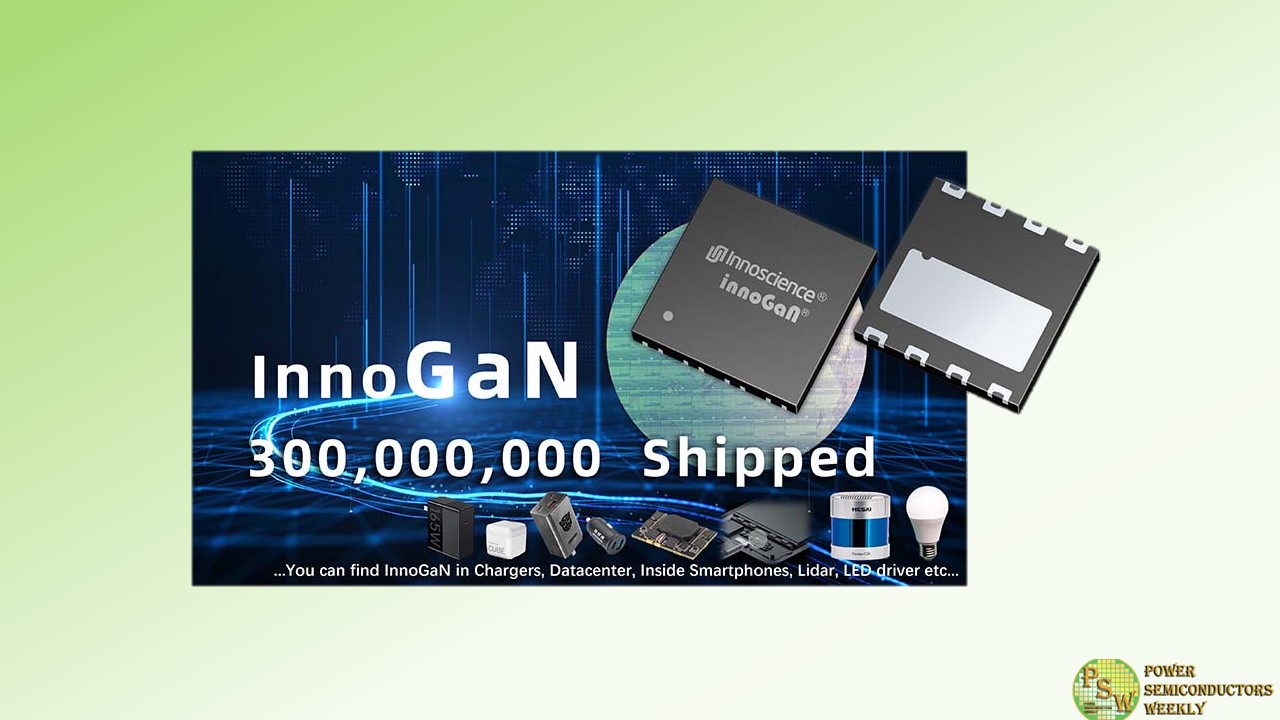
Innoscience Technology has shipped more than 300 million pieces of its InnoGan gallium nitride chips as of August 2023, helping customers achieve small size, high energy efficiency, and low loss product design.
This is in response to phenomenal market demand across multiple sectors multiple applications in the consumer category – fast charging, mobile phones, LEDs – as well as automotive LIDAR, data centres, and renewable energy and energy storage systems, which has seen analysts such as TrendForce’s in its 2023 GaN Power Semiconductor Market Analysis Report, state that “the global GaN power device market will grow from US$180 million in 2022 to US$1.33 billion in 2026, with compound growth rate of 65%”.
In November 2017, Innoscience began the world’s first 8-inch GaN-on-Si mass production line, adopting the Integrated Device Manufacturer (IDM) whole industry chain model, and launched its first low-voltage GaN power device in May 2018. By June 2019, Innoscience’s 650V high-voltage GaN device had passed JEDEC approval, and subsequently, Innoscience has been the only semiconductor company in the world that simultaneously mass-produces high-voltage and low-voltage GaN.
Market acceptance of Innoscience’s high quality, high performance GaN devices has been swift. Following its 2019 entry into the fast charging market, Innoscience’s 650V parts have been adopted in 30W-120W designs by leading brands including ASUS, Anker, Nubia, Baseus, Greenlink, and Flash.
In 2020, Innoscience’s 100V low-voltage GaN was successfully used by Hesai in mass-production LIDAR designs, allowing lasers to achieve image transmission in a shorter time.
In March 2021, the Tencent×Nubia Red Magic mobile phone 6Pro was released. It comes equipped as standard with industry’s first 120W Black Rubik’s Cube GaN fast charge, which is based on Innoscience’s 650V chip. With the successive adoption by Oppo, Vivo, Lenovo and other manufacturers, it has become an industry trend for mobile phones to be equipped with GaN fast charging as standard.
March 2021 saw the mass-production of Innoscience’s bi-directional conduction chip V-GaN officially begin; this device is the only GaN chip in the world that can be applied to high-voltage side load switches, smartphone USB/wireless charging ports with built-in OVP protection, multi-power supply system switch circuits, and other scenarios:one V-GaN replaces two Si MOSFETs in load switching applications resulting in a smaller and more efficient solution.
In October of the same year, Innoscience scored another industry first, as OPPO used the company’s self-developed bi-directional conduction VGaN IC as the internal power switch in its latest smart phone. Other mobile phone makers such as Realme, OnePlus, Lenovo, and Motorola have also successively adopted VGaN for charging protection.
In May 2022, Shounuo released the world’s smallest 45W/65W PD car charger, using Innoscience’s 40V low-voltage INN040FQ043A.
Then in July, Anker and Innoscience jointly released the world’s first 65W full-GaN fast charger. This design uses GaN power chips at both the AC and DC ends for the first time, taking system power density and efficiency to a whole new level.
Later, in October 2022, Innoscience achieved mass production of GaN products targeting industrial power supplies – again an industry first – comprehensively improving energy conversion efficiency and reducing system energy consumption.
In November 2022, Innoscience’s INN100W032A won the IIC World Electronics Achievement Award. The gate charge of this product is only 20% of a traditional silicon MOSFET, and its Ciss is only 40% of its silicon counterpart. It can be widely applied in motor drive, Class D, data centre, motor-driver, communication base station and other product fields. In January 2023, Innoscience launched the SolidGaN ISG3201, a 100V highly-integrated half-bridge drive packaged solution, further improving the overall system performance of 48V power supply of data centre module power supplies, motor drives, class D power amplifiers, photovoltaic inverters and light hybrid electric vehicles.
The move to GaN as the premium power semiconductor technology is driven both by new GaN products and market demands. As an example, in April this year, Innoscience’s IATF 16949 automotive-grade low-voltage parts successfully expanded from industrial to automotive applications, with use in autonomous vehicle LIDAR systems.
Then in July 2023, Innoscience began to apply GaN in the field of renewable energy, reducing the size and improving the efficiency of photovoltaic modules.
By the end of August 2023, Innoscience had successfully mass-produced 54 different types of high-voltage GaN chips (650V-700V) and 20 types of medium-low voltage GaN chips (30V-150V). Products span three chip categories: wafers, discrete devices and integrated solutions.
Commented Dr Denis Marcon, Innoscience’s General Manager, Europe: “We are just at the start of the GaN story. The first applications were all in consumer, but GaN is undoubtedly the key to reducing costs and increasing efficiency in the industrial field as well. And according to automotive industry forecasts, GaN may enter automotive market already this year penetrating applications such as low-power OBC and DC-DC applications in 2025.
With such rapid growth in market demand, the reliability of devices, price competitiveness and stable supply in large quantities are now the major concerns of users. Based on an advanced Innoscience’s 8-inch GaN-on-Si IDM manufacturing platform, Innoscience’s current production capacity has reached 15,000 wafers per month, providing tremendous advantages in scale, reliability and cost.”
Original – Innoscience Technology
