-
Navitas Semiconductor announced participation at the International Conference on Silicon Carbide and Related Materials (ICSCRM) 2023, to be held in Sorrento, Italy.
The ICSCRM conference fosters collaboration and knowledge sharing among the brightest minds in the field. The conference has a rich history dating back to its inaugural meeting in 1987, evolving into a premier global forum for in-depth technical discussions on all aspects of SiC and related materials.
GeneSiC™ power devices, optimized for high-power, high-voltage, and high-reliability SiC applications, address critical markets including electric vehicles, solar energy, energy storage, industrial applications, data centers, and consumer electronics. With an unmatched voltage range spanning from 650 V to 6.5 kV, GeneSiC MOSFETs and Schottky MPS™ diodes have been at the forefront of SiC technology advancement, offering performance and efficiency that pave the way for a more electrified and sustainable future.
Navitas Semiconductor will present two paper sessions at ICSCRM 2023:
- “New Generation SiC MPS Diodes with Low Schottky Barrier Height”
- “650 V SiC Power MOSFETs with Statistically Tight VTH Control and RDS(ON) of 1.92 mΩ-cm²”
Additionally, Navitas’ SVP of SiC Technology & Operations, Dr. Sid Sundaresan, will be chairing the session on Thursday, September 21st. The session, titled “Devices 4: Short circuit, avalanche and reliability,” will focus on crucial topics in the field of SiC technology.
“Navitas’ presence at ICSCRM 2023 is a testament to the company’s unparalleled expertise in SiC technology and its commitment to driving innovation in the industry,” said Dr. Ranbir Singh, Navitas EVP for the GeneSiC business line. “As a pioneer in the field, we continue to extend the boundaries of SiC technology, revolutionizing power semiconductors with cutting-edge GeneSiC™ technology.”
Original – Navitas Semiconductor
-
Navitas Semiconductor will reveal a new, high-performance wide bandgap power platform as part of its display at one of Asia’s most prestigious electronics exhibitions – sponsored by Navitas – SEMICON Taiwan 2023, from September 6th-8th.
Visitors will discover the latest gallium nitride (GaN) GaNFast™ power ICs integrate gallium nitride (GaN) power and drive, with control, sensing, and protection to enable faster charging, higher power density, and greater energy savings. Complementary GeneSiC™ power devices are optimized high-power, high-voltage, and high-reliability silicon carbide (SiC) solutions.
Additionally, Navitas will showcase cutting-edge, power-system platforms to dramatically accelerate customer developments, minimize time-to-market, and set new industry benchmarks in energy efficiency, power density and system cost. These system platforms include complete design collateral with fully-tested hardware, embedded software, schematics, bill-of-materials, layout, simulation and hardware test results. Examples include:
- Navitas’ CRPS185 data center power platform, that delivers a full 3,200 W of power in only 1U (40 mm) x 73.5mm x 185 mm (544 cc), achieving 5.9 W/cc, or almost 100 W/in3 power density. This is a 40% size reduction vs, the equivalent legacy silicon approach and reaches over 96.5% efficiency at 30% load, and over 96% stretching from 20% to 60% load, creating a ‘Titanium Plus’ benchmark.
- Navitas’ 6.6 kW 3-in-1 bi-directional EV on-board charger (OBC) with 3 kW DC-DC. This 96%+ efficient unit has over 50% higher power density, and with efficiency over 95%, delivers up to 16% energy savings as compared to competing solutions.
As part of SEMICON’s Power and Opto Semiconductor Forum, Navitas’ Charles Bailley, Senior Director of Business Development, will present “GaN Power ICs Increase Power Density in EV Power Systems”. The presentation is at 2pm, on September 6th, in room 402, 4F, TaiNEX 1.
“Breakthrough high efficiency, high reliability, and high power density – all from the new GaN power IC platform,” said Kevin 汪時民 Wang, Manager of Navitas Taiwan. “The new platform announcement matches SEMICON’s theme of ‘Innovating the World through Semiconductors’ and our own mission to ‘Electrify Our World™’.”
Original – Navitas Semiconductor
-
Navitas Semiconductor and Plexim GmbH announced a partnership to release GeneSiC G3™ SiC MOSFET and Gen 5 MPS diode PLECS thermal loss models for highly-accurate simulations of complete power electronics systems.
Power designers can simulate power and thermal losses in various soft- and hard-switching applications. Proprietary GeneSiC trench-assisted planar-gate MOSFET technology delivers the lowest RDS(ON) at high temperature and the highest efficiency at high speeds, and new MPS diodes with ‘low-knee’ characteristics drive unprecedented, industry-leading levels of performance, robustness and quality.
“Accurate, empirically-based simulation models maximize the chance of first-time-accurate designs, accelerating time-to-market and time-to-revenue,” noted Dr. Ranbir Singh, Navitas EVP for the GeneSiC business line. “For the power designer, understanding the leading-edge performance of GeneSiC MOSFETs and MPS diodes with detailed device characteristics, plus power, efficiency and thermal analysis is a critical competitive advantage.”
“The intuitive and highly-efficient PLECS lookup-table based approach to simulating thermal semiconductor losses in complex power electronic circuits is key,” said Kristofer Eberle, Plexim, North America. “Unlike legacy modeling approaches that are not well-suited to new wide bandgap materials, PLECS uses a simplified, but accurate behavioral description to highlight the superior performance of the GeneSiC MOSFETs.”
PLECS models for GeneSiC MOSFETs and MPS diodes are available via genesicsemi.com.
Original – Navitas Semiconductor
-
 LATEST NEWS / PRODUCT & TECHNOLOGY / SiC / TOP STORIES / WBG
Navitas Launches into High-Power Markets with GeneSiC SiCPAK™ Modules and Accelerates Bare-Die Sales
May 8, 2023
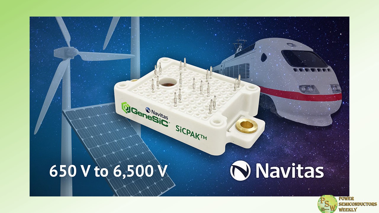
2 Min ReadNavitas Semiconductor, the only pure-play, next-generation power semiconductor company, announced their expanded portfolio into higher power markets with their leading-edge silicon carbide (SiC) power products in SiCPAK™ modules and bare die.
Target applications cover centralized and string solar inverters, energy storage systems (ESS), industrial motion, electric vehicle (EV) on-board chargers, EV roadside fast chargers, wind energy, UPS, bi-directional microgrids, DC-DC converters, and solid-state circuit breakers.
Ranging from 650 V to 6,500 V, Navitas has the widest range of SiC technology. From an original line-up of discrete packages – from 8×8 mm surface-mount QFNs to through-hole TO-247s – the GeneSiC SiCPAK is an initial, direct entry point into higher-power applications. A comprehensive power-module roadmap, with high-voltage SiC MOSFETs and MPS diodes, GaN power ICs, high-speed digital isolators and low-voltage silicon control ICs is being mapped out.
Dr. Ranbir Singh, Navitas EVP for SiC noted, “With a complete portfolio of leading-edge power, control and isolation technology, Navitas will enable customers to accelerate the transition from fossil fuels, and legacy silicon power products to new, renewable energy sources and next-generation semiconductors, with more powerful, more efficient, faster-charging systems.”
SiCPAK™ modules employ ‘press-fit’ technology to offer compact form factors for power circuits and deliver cost-effective, power-dense solutions to end users. The modules are built upon GeneSiC die that have already made a mark in terms of superior performance, reliability, and ruggedness. Examples include a SiCPAK half-bridge module, rated at 6 mOhm, 1,200 V with industry-leading trench-assisted planar-gate SiC MOSFET technology. Multiple configurations of SiC MOSFETs and MPS diodes will be available to create application-specific modules for superior system performance. The initial release will include 1,200 V-rated half-bridge modules in 6, 12, 20, and 30mOhm ratings.
Within the lead-free SiCPAK, each SiC chip is silver (Ag) sintered to the module’s substrate for superior cooling and reliability. The substrate itself is ‘direct-bonded copper’ (DBC) and manufactured using an active-metal brazing (AMB) technique on silicon-nitride (Si3N4) ceramics, ideal for power-cycling applications. This construction delivers excellent strength and flexibility, fracture resistance, and good thermal conductivity for cool, reliable, long-life operation.
For customers who prefer to make their own high-power modules, all GeneSiC MOSFET and MPS diodes are available in bare die format, with gold (Au) and aluminum (Al) top-side metalizations.
Original – Navitas Semiconductor

