-

Alpha and Omega Semiconductor Limited announced the expansion of their package portfolio options available for their second generation 650V to 1200V αSiC MOSFETs. Applicable to many critical applications such as xEV charging, solar inverters, and industrial power supplies, the new package selections give designers the added flexibility of multiple system optimization options to further maximize system efficiency while streamlining their manufacturing process.
AOS will showcase its expanded surface mount and module package options at PCIM Europe 2024 in Nuremberg, Germany, June 11-13.
The first new surface mount package is available for the AOBB040V120X2Q, AOS’ new 1200V/40mOhm αSiC MOSFET in a standard D2PAK-7L surface mount package. This AEC-Q101 qualified product is designed to replace traditional through-hole packages. It is ideal for applications such as on-board chargers (OBCs) where efficient cooling can be provided by vias and backside PCB heatsinks, simplifying the assembly flow and maximizing the power density. In addition, the low inductance package combined with the fast driver sourcesense connection positions these AOS αSiC MOSFETs as one of the most efficient power-switching solutions in the market.
For additional design flexibility, AOS is releasing its GTPAK™ surface mount package with topside cooling features. In designs where a topside-mounted heatsink is viable, the direct heat path from the GTPAK minimizes the thermal resistance. It enables higher power dissipation for more effective PCB routing. The first AOS product in GTPAK is the AOGT020V120X2. This 1200V/20mOhm αSiC MOSFET is an ideal solution to meet the requirements of high-efficiency solar inverter and industrial power supply applications.
Finally, AOS announced the AOH010V120AM2 as the first product in its new AlphaModule™ high power baseplate-less module family. This 1200V/10mOhm half-bridge αSiC module features press-fit pins and an integrated thermistor. It is in a standard footprint module that enables the replacement of multiple discrete devices into a single compact form factor while simplifying both the mechanical and electrical design by providing a clear separation of electrical and cooling paths. Single modules are suitable for residential solar inverters, or several modules in parallel will allow scaling to power levels necessary to drive the needs of fast DC charging stations.
“With the continued growth in EVs, energy infrastructure, and renewable energy, we continue to see increased interest in our αSiC MOSFETs. The expansion of our product portfolio to include these new advanced package options gives our customers the design flexibility they need to take advantage of our superior αSiC performance and continue the trend of pushing power systems to higher density and efficiency,” said David Sheridan, Vice President of SiC products at AOS.
Original – Alpha and Omega Semiconductor
-

Alpha and Omega Semiconductor Limited (AOS) will showcase its expanding line of advanced power management solutions at PCIM 2024. Designed to meet the dynamic, important power management challenges in several key application areas and markets, the AOS products highlighted at PCIM include:
- New Silicon Carbide (SiC) MOSFET Announcement at PCIM: Supporting the needs of a wide range of automotive and industrial applications, AOS will introduce three new advanced package options for its latest Gen2 SiC MOSFET line. The new packages comprise a surface mount topside cooling option with a Kelvin source that meets the needs of the most power-dense advanced designs. It will also be announced that an AEC-Q101-qualified surface mount package will be in the standard D2PAK-7L footprint. The third package is a half-bridge module that provides an excellent solution for the high power industrial solar and charging station markets. The announcements will detail how these packages support AOS’ comprehensive line of SiC MOSFETs from 10mOhm to 500mOhm and voltages from 650V to 1700V.
- New Motor Drive Announcement at PCIM: AOS will announce a new range of 60V and 100V drivers for power tools, outdoor garden equipment, and e-mobility applications, including a 100V half bridge, a 100V 3-phase, and a 60V 3-phase. These products all support 100 percent duty cycle operation, and demo boards using AOS motor drivers and MOSFETs will be featured in the AOS booth.
- Power Supply and Renewable Energy: A significant solution in AOS’ growing High Voltage Super Junction MOSFET portfolio is its industry-leading optimized αMOS5™ 600V to 700V Super Junction MOSFETs that help designers achieve efficiency and density goals while satisfying budget goals. Featuring fast switching, a robust UIS/body diode, and ease of use, these state-of-the-art MOSFETs meet the latest server, telecom rectifier, solar inverter, EV charger, gaming, PC, and universal charging/PD design requirements. The newly released AONA66916, a 100V AlphaSGT™ MOSFET, delivers industry-leading Rthjc-top and Rthjc-bottom thermal resistances. A compact DFN 5×6 double-sided cooling package offers improved thermal designs in demanding telecom, solar, and DC-DC converter applications.
- Automotive and E-mobility: In AOS’ increasing line of automotive MOSFETs, the new automotive grade 80V (AOTL66810Q) and 100V (AOTL66912Q) MOSFETs in the TOLL package are designed to achieve the highest current capability. The AOS TOLL package utilizes advanced clip technology to achieve a high in-rush current rating and very low package resistance and inductance, enabling improved EMI performance compared to other TOLL packages based on standard wire-bonding technology packages. These new automotive-grade MOSFETs help designers meet the power requirements in electric vehicles, battery management systems (BMS), and high-performance inverters (BLDC motors) for e-mobility.
- Intelligent Power Modules, Mega IPM7: AOS has integrated its latest RC IGBT and high-voltage gate driver into the world’s most compact package design, capable of delivering mega power of up to 100W in motor control applications. The portfolio covers 600V / (1A−3A) in a variety of package options (Mega IPM-7D, IPM7DT, IPM-7E) that are ideal solutions for a broad array of design requirements.
- Poster Presentation: Jong-Mu Lee, Ph.D. and director of AOS IGBT and Module Product Lines, will present SiC-IPM for Compact and Energy Efficient in the Intelligent Power Modules session on Tuesday, June 11, at 15:30.
Original – Alpha and Omega Semiconductor
-

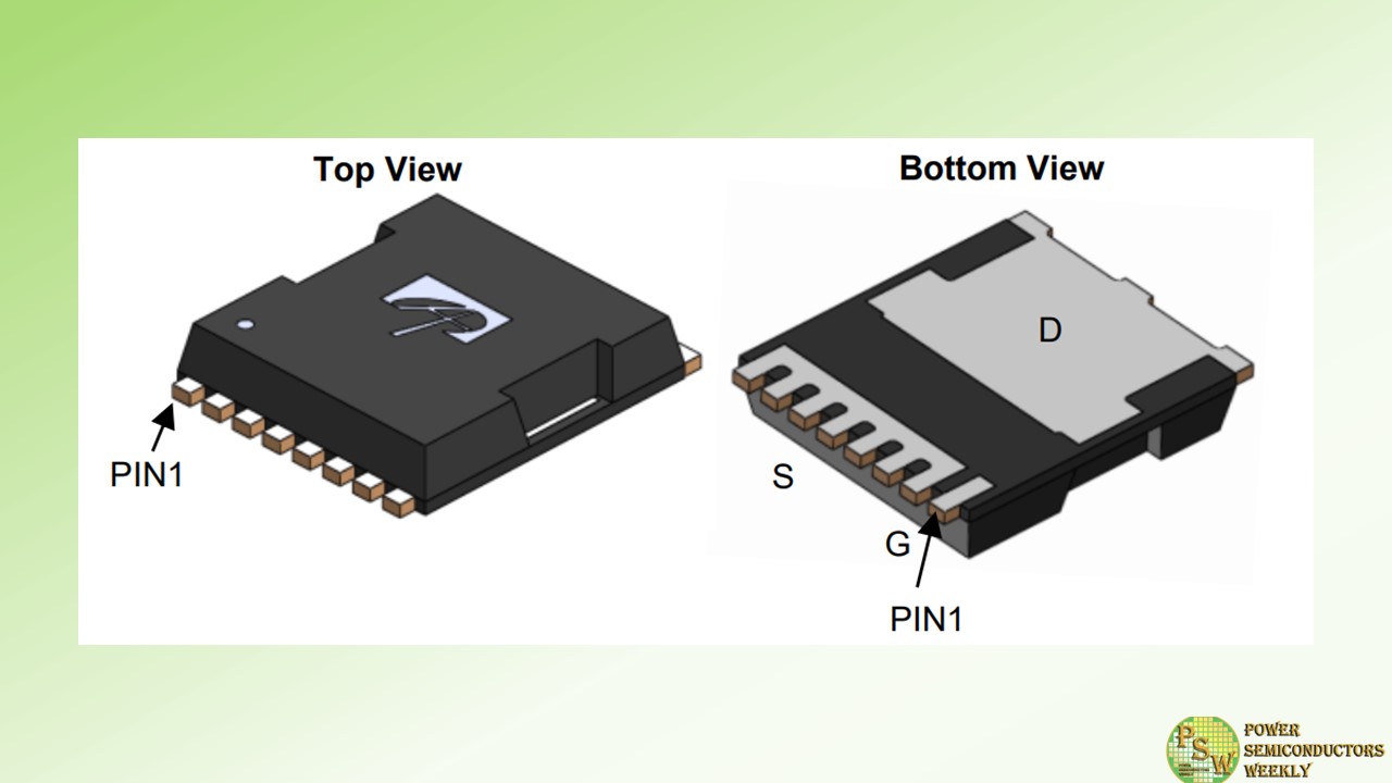
Alpha and Omega Semiconductor Limited announced its AONZ66412 XSPairFET™ MOSFET designed for Buck-Boost converters in USB PD 3.1 Extended Power Range (EPR) applications. The USB PD 3.1 EPR increases the USB-C maximum power up to 240W. AONZ66412 is defined to support the most commonly addressed power range of up to 140W at 28V, with two 40V N-Channel MOSFETs in a half-bridge configuration in a symmetric XSPairFET™ 5mmx6mm package.
The AONZ66412 can replace two single DFN5x6 MOSFETs, reducing the PCB area and simplifying the layout of the 4-switch buck-boost architecture while enabling a higher efficiency design. These benefits make the AONZ66412 ideal for buck-boost converters in Type-C USB 3.1 EPR applications, including notebook, USB hub, and power bank designs. The AONZ66412 is an extension to the AOS XSPairFET™ lineup that features the latest bottom source packaging technology and lower parasitic inductance for reduced switch node ringing.
Engineered with integrated high-side and low-side MOSFETs (3.8mOhms maximum on-resistance for each FET) within a DFN5x6 symmetric XSPairFET™ package, the low-side MOSFET source of the AONZ66412 is connected directly to a large paddle on the lead frame. This allows for improved thermals, as this paddle can be directly connected to the ground plane on the PCB. The improved package parasitics make 1MHz operation achievable, allowing inductor size and height to be reduced. AONZ66412 has been tested to achieve 97% efficiency @1MHz in typical USB PD 3.1 EPR conditions of 28V input, 17.6V output, and 8A load conditions.
“AOS specifically designed the AONZ66412 to meet EPR Type C PD application demands. AONZ66412 will reduce board space and improve power density to achieve the high-efficiency performance goals designers have set for this widely adopted USB-PD Type C application. AOS continues to be a leading innovator of buck-boost architecture solutions,” said Rack Tsai, Marketing Director of MOSFET product line at AOS.
Original – Alpha and Omega Semiconductor
-
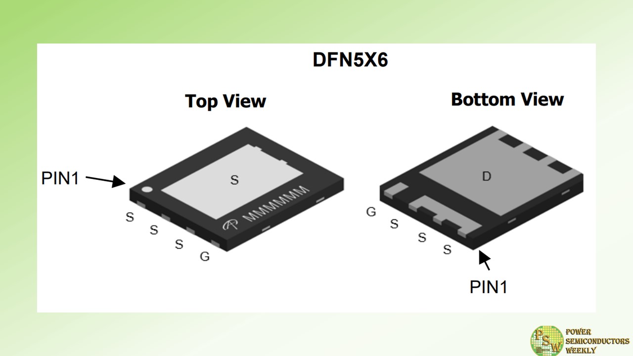
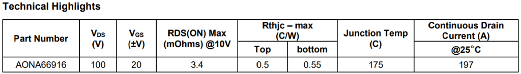
Alpha and Omega Semiconductor Limited (AOS) announced the AONA66916, a 100V MOSFET packaged in the company’s innovatively designed top and bottom side cooling DFN 5 x 6 package. Designers have long trusted AOS power semiconductors as essential components that help them meet a wide variety of high performance application requirements.
Now, in delivering a state-of-the-art package that keeps its semiconductor products cooler, AOS is taking a huge step in enabling engineers to develop more efficient designs in telecommunications and industrial applications that must frequently operate in harsh conditions.
Typically, when using the standard DFN 5×6 package, the bottom contact is the main contributor for cooling, and most of the heat generated by the Power MOSFETs will be transferred to the PCB. This increases the PCB thermal management design considerations to meet system requirements. AOS’ new top and bottom cooling DFN 5×6 package is designed to achieve the highest heat transfer between the exposed top contact and heat sink due to its large surface contact area construction.
This allows the device to achieve a low thermal resistance (Rthc-top max) of 0.5°C / W with results being transferred to the PCB board, enabling significant thermal performance improvements. The top exposed DFN 5×6 package of the AONA66916 shares the same 5mm x 6mm footprint as AOS’ standard DFN 5×6 package, eliminating the need to modify existing PCB layouts.
Another benefit of the AONA66916 is that it utilizes AOS’ 100V AlphaSGT™ technology, providing excellent FOM for balanced performance in hard switching applications. AONA66916 has a maximum RDS(on) rating of 3.4mOhms and has a 175°C junction temperature rating.
“Cooling the power MOSFET in high power design can be challenging, and AOS has successfully addressed this essential issue with our advanced top exposed package design. It not only enables better thermal transfer from its top side exposed contact to heat sink due to large exposed surface area, our new package delivers a much cooler device that contributes to a more efficient and robust final design,” said Peter H. Wilson, Marketing Sr. Director of the MOSFET product line at AOS.
Original – Alpha and Omega Semiconductor
-

Alpha and Omega Semiconductor Limited announced the release of two αMOS5™ 600V FRD Super Junction MOSFETs. αMOS5™ is AOS’s market and application-proven high voltage MOSFET platform, designed to meet the high efficiency and high-density needs of servers, workstations, telecom rectifiers, solar Inverters, EV charging, motor drives and industrial power applications.
The design of today’s mid-high power switched-mode power supply (SMPS) and solar inverter systems boil down to four major challenges – higher efficiency, higher density, lower system costs, and uncompromised robustness. High Voltage Super Junction MOSFETs are dominant the choice for topologies such as single/interleaved/dual boost/CrCM TP PFCs, LLC, PSFB, multi-level NPC/ANPC and so forth.
αMOS5™ has been the leading High Voltage Super Junction solution tailored for fast switching, ease-of use and robustness in mission-critical applications. αMOS5™ FRD FETs are engineered with strong intrinsic body diode to handle hard commutation scenarios, when the freewheeling body diode is in reverse recovery due to abnormal operations, such as short-circuit or start-up transients.
The two products released, the AOK095A60FD (TO-247) and AOTF125A60FDL (TO-220F), are 600V FRD FETs with 95mohm and 125mohm maximum Rdson, respectively. In tests conducted by AOS engineers, the body diodes of these two FRD FETs have survived high di/dt, under abnormal system conditions, even at elevated junction temperatures of up to 150°C. Additionally, AOS tests have shown that these devices’ turn off energy (Eoff) are noticeably lower than the competition’s, which contributes to higher efficiency in light or mid-load conditions.
“We defined our products for traditional power supplies, as well as DC/DC and DC/AC converters of solar inverters and ESS systems, where bi-directional topologies are needed. As energy storage-ready inverters become the trend and high voltage batteries are utilized increasingly in AC-coupled systems, the AOK095A60FD and AOTF125A60FDL will become industry leading solutions for bi-directional DC/DC and inverter/PFC applications that serve a wide range of power supplies, solar PV inverters, and ESS hybrid converters,” said Richard Zhang, Senior Director of Product Line and Global Power Supply Business at AOS.
Technical Highlights
- Rugged, fast recovery diode (FRD) with reduced Qrr for demanding use cases
- Engineered for both hard and soft switching topologies with ultra-low switching loss
- Strong UIS and SOA capabilities
- Engineered to prevent self turn-on
- Suitable for LLC, PSFB, CrCM Totem-Pole, Multi-level NPC and CrCM H-4/Cyclo Inverter applications
Original – Alpha and Omega Semiconductor
-
Alpha and Omega Semiconductor Limited (AOS) announced the release of its state-of-the-art automotive TO-Leadless (TOLL) package for the company’s automotive grade 80V and 100V MOSFETs. AOS’s TOLL package is developed to optimize the company’s power semiconductors as essential components in the evolution of e-mobility such as 2- and 3-wheel and other light vehicles. This new package helps designers meet the ongoing trend to electrify vehicles with the latest battery technology to meet clean energy zero-emission goals.
These capabilities make AOS 80V and 100V MOSFETs ideally suited for automotive BLDC motor and battery management applications for e-mobility. The AOS automotive TOLL package is designed to achieve the highest current capability using AOS’s innovative approach which utilizes advanced clip technology to achieve a high in-rush current rating.
In addition, AOS TOLL packaging with clip technology offers a very low package resistance and inductance, enabling improved EMI performance compared to other TOLL packages utilizing standard wire-bonding technology. With the combination of low ohmic and high current capability, utilizing AOS TOLL packaging also allows designers to reduce the number of parallel MOSFETs in high current applications. This, in turn, helps to enable higher power density requirements without compromising reliability in applications where robustness and reliability are key design objectives.
Providing a more compact solution for space-constrained designs, the AOTL66810Q (80V) and AOTL66912Q (100V) have a 30 percent smaller footprint compared to a TO-263 (D2PAK) package. These new devices in TOLL packaging are qualified to AEC-Q101, PPAP capable, and are manufactured in IATF 16949 certified facilities making them ideally suited for demanding application requirements in e-mobility. AOS TOLL devices are also compatible with automated optical inspection (AOI) manufacturing requirements.
“Using the AOS Automotive TOLL package with clip technology offers significant performance improvements in a robust package. The advanced technologies in our AOTL66810Q and AOTL66912Q MOSFETs will help simplify new designs allowing them to reduce the number of devices in parallel while providing the necessary higher current capability to enable overall system cost savings,” said Peter H. Wilson, Marketing Sr. Director of MOSFET product line at AOS.
Part Number VDS (V) VGS (±V) Continuous Drain Current (A) Pulsed Drain Current (A) RDS(ON) Max (mOhms) @10V @25°C @100°C @25°C AOTL66810Q 80 20 445 247 1780 1.25 AOTL66912Q 100 20 370 269 1480 1.7 Original – Alpha and Omega Semiconductor
-
Alpha and Omega Semiconductor Limited (AOS) announced the release of 600V αMOS7™ Super Junction MOSFETs Family. αMOS7™ is AOS’ next generation high voltage MOSFET, designed to meet the high efficiency and high-density needs of servers, workstations, telecom rectifiers, solar Inverters, EV charging, motor drives and industrial power applications.
Today’s Server power supply requires Titanium efficiency, which translates to more than 98.5% peak efficiency on both PFC and LLC stages. Active-Bridges and Bridgeless designs are easy-to-implement solutions; however, switching and driving losses, especially at light load, are still the main problems designers face. Existing technologies limited by large cell pitches and charges could hardly meet such requirements.
Next-gen SJ technologies with reduced charge but also enough robustness is in demand. Low Qrr and Trr for LLC and PSFB applications are also a must during transient and abnormal situations. AOS αMOS7™ High Voltage SJ MOSFET is the best answer for above needs.
For Solar applications, low ohmic SMD devices are becoming the new standards, aiming for reduced form factors through utilizing 3D mechanical and thermal designs. αMOS7™ provides a wide Rdson granularity and SMD package choices, such as DFN, TOLL, and Top-cooling variants.
For low Fsw applications such as Solid-State Relays or Active Bridges, FETs must meet specific SOA requirements to sustain surge and in-rush currents. αMOS7™ ensures low Rdson’s temperature coefficient and ruggedness for transient voltage and current overstresses.
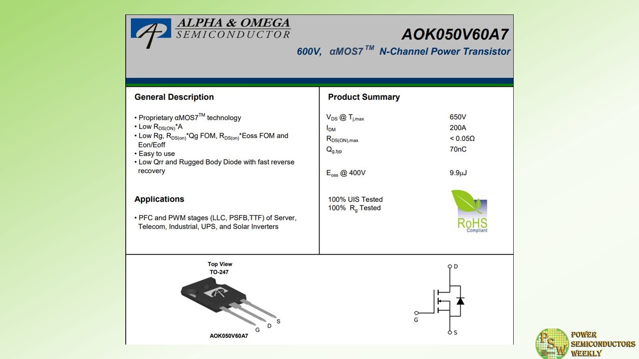
The first product released – AOK050V60A7 is a 600V 50mOhm αMOS7 low ohmic device with the industry-standard TO-247 package tailored for today’s high-power AC/DC, DC/DC, and Solar Inverter stages. As the EU ERP Lot9 regulation pushes the efficiency of single PSUs to Titanium level, AOS αMOS7™ 600V low ohmic family provides an ideal solution for single, interleaved, dual boost, totem-pole, and Vienna PFCs, as well as other hard-switching topologies. The optimized capacitance of AOK050V60A7 will provide customers excellent switching performances, with fast turn-on/turn-off behaviors, while avoiding the risks of self-turn-on or shoot-through. The 50mohm device will be followed by our upcoming 32mohm, 40mohm, 65mohm, and 105mohm devices.
“The new charge balance structure makes it possible to further reduce the active area up to 50%, compared to αMOS5™, our existing solution. In general, αMOS7™ is an industry-leading high voltage SJ solution designed to address both efficiency driven and cost-driven markets,” said Richard Zhang, Senior Director of Product Line and Global Power Supply businesses at AOS.
Technical Highlights:
- Low Ohmic device with ultra-low switching losses
- Rugged Body Diode and FRD options (Reduced Qrr) available for more demanding use cases
- Rugged SOA and in-rush current capability for Solid-State Relay and Active Bridge applications
- Optimized for both High Power and Low Power SMPSes, Solar Inverters, and EV DC Charging applications
Original – Alpha and Omega Semiconductor
