-

Infineon Technologies AG is revolutionizing the power delivery architecture required for future AI data centers. In collaboration with NVIDIA, Infineon is developing the next generation of power systems based on a new architecture with central power generation of 800 V high-voltage direct current (HVDC).
The new system architecture significantly increases energy-efficient power distribution across the data center and allows power conversion directly at the AI chip (Graphic Processing Unit, GPU) within the server board. Infineon’s expertise in power conversion solutions from grid to core based on all relevant semiconductor materials silicon (Si), silicon carbide (SiC) and gallium nitride (GaN) is accelerating the roadmap to a full scale HVDC architecture.
This revolutionary step paves the way for the implementation of advanced power delivery architectures in accelerated computing data centers and will further enhance reliability and efficiency. As AI data centers already are going beyond 100,000 individual GPUs, the need for more efficient power delivery is becoming increasingly important. AI data centers will require power outputs of one megawatt (MW) and more per IT rack before the end of the decade. Therefore, the HVDC architecture coupled with high-density multiphase solutions will set a new standard for the industry, driving the development of high-quality components and power distribution systems.
“Infineon is driving innovation in artificial intelligence,” said Adam White, Division President Power & Sensor Systems at Infineon. “The combination of Infineon’s application and system know-how in powering AI from grid to core, combined with NVIDIA’s world-leading expertise in accelerated computing, paves the way for a new standard for power architecture in AI data centers to enable faster, more efficient and scalable AI infrastructure.”
“The new 800V HVDC system architecture delivers high reliability, energy-efficient power distribution across the data center,” said Gabriele Gorla, vice president of system engineering at NVIDIA. “Through this innovative approach, NVIDIA is able to optimize the energy consumption of our advanced AI infrastructure, which supports our commitment to sustainability while also delivering the performance and scalability required for the next generation of AI workloads.”
At present, the power supply in AI data centers is decentralized. This means that the AI chips are supplied with power by a large number of power supply units (PSU). The future system architecture will be centralized, making the best possible use of the constraint space in a server rack. This will increase the importance of leading-edge power semiconductor solutions using fewest power conversion stages and allowing upgrades to even higher distribution voltages.
Infineon is a leader in power semiconductor solutions and systems integration. The company expects the proportion of power semiconductors in a centralized HVDC architecture to be similar or higher than in today’s AC distribution architecture. Additionally, to the scaling of the HVDC power architecture, Infineon continues to support state of the art DCDC multiphase solutions and intermediate architectures for hyperscalers and AI data center operators with a broad product portfolio based on all relevant semiconductor materials along the entire power flow.
Learn more about Infineon’s AI power and data center solutions here.
Original – Infineon Technologies
-

Toshiba Electronic Devices & Storage Corporation (“Toshiba”) has launched four 650V silicon carbide (SiC) MOSFETs, equipped with its latest 3rd generation SiC MOSFET chips and housed in a compact DFN8×8 package, suitable for industrial equipment, such as switched-mode power supplies and power conditioners for photovoltaic generators. Volume shipments of the four devices, “TW031V65C,” “TW054V65C,” “TW092V65C,” and “TW123V65C,” start today.
The new products are the first 3rd generation SiC MOSFETs to use the small surface-mount DFN8×8 package, which reduces volume by more than 90% compared to lead-inserted packages, such as TO-247 and TO-247-4L(X) and improves equipment power density. Surface mounting also allows use of parasitic impedance components smaller than those of lead-inserted packages, reducing switching losses.
DFN8×8 is a 4-pin package, allowing use of a Kelvin connection of its signal source terminal for the gate drive. This reduces the influence of inductance in the source wire within the package, achieving high-speed switching performance; in the case of TW054V65C, it reduces turn-on loss by approximately 55% and turn-off loss by approximately 25% compared to current Toshiba products, helping to reduce power loss in equipment.
Toshiba will continue to expand its lineup to contribute to improved equipment efficiency and increased power capacity.
Applications
- Switched mode power supplies in servers, data centers, communications equipment, etc.
- EV charging stations
- Photovoltaic inverters
- Uninterruptible power supplies
Features
- DFN8×8 surface-mount package. Enables equipment miniaturization of and automated assembly. Low switching loss.
- Toshiba’s 3rd generation SiC MOSFETs
- Good temperature dependence of drain-source On-resistance by optimization of drift resistance and channel resistance ratio
- Low drain-source On-resistance×gate-drain charges
- Low diode forward voltage: VDSF=-1.35V(typ.) (VGS=-5V)
Original – Toshiba
-
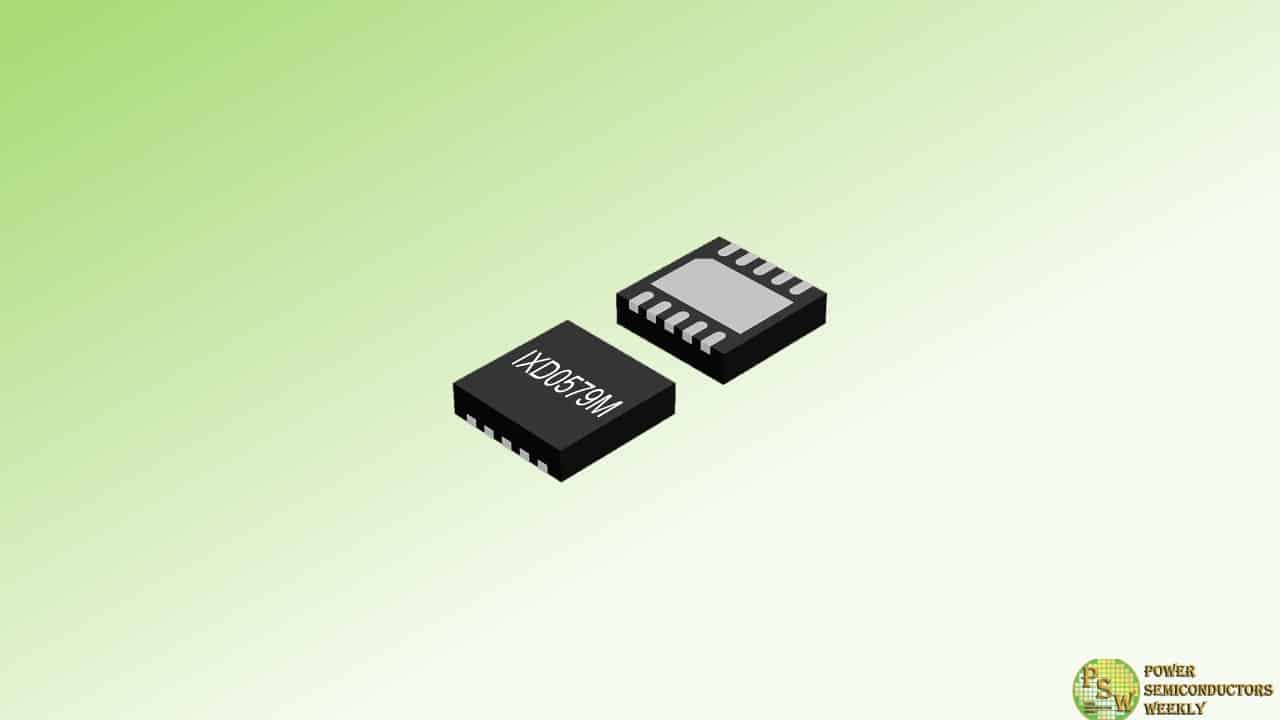
Littelfuse, Inc. announced the release of the IXD0579M high-speed gate driver IC. The IXD0579M simplifies board design, saves space, and offers a reliable, multiple-source alternative for driving N-channel MOSFETs or IGBTs in half-bridge configurations.
Designed to operate across a wide 6.5 V to 18 V supply range, the IXD0579M integrates a bootstrap diode and a series current limit resistor—components typically requiring discrete placement—into a single compact 3×3 mm² TDFN-10 package. This innovative integration reduces BOM count and cost while enabling easier PCB layout.
Key Product Features and Benefits
- High Drive Capability: 1.5 A source and 2.5 A sink output drive current
- Wide Supply Voltage Range: Operates from 6.5 V to 18 V with UVLO protection
- Integrated Bootstrap Circuitry: On-chip bootstrap diode and resistor simplify design
- Logic Level Compatibility: Interfaces directly with TTL and CMOS levels (down to 3.3 V)
- Cross-Conduction Protection: Prevents simultaneous high-side and low-side conduction
- Ultra-Low Standby Current: Less than 1 µA standby mode for energy efficiency
- Thermal Robustness: Operates from −40 °C to +125 °C
“With the IXD0579M, Littelfuse is offering a direct drop-in replacement for popular industry-standard gate driver ICs,” said June Zhang, Product Manager, Integrated Circuits Division at Littelfuse. “This gives customers greater flexibility to secure supply while simplifying their circuit design with an integrated solution.”
The IXD0579M is the first Littelfuse gate driver to feature both an integrated bootstrap diode and current limit resistor, expanding the company’s growing portfolio of power control solutions. As the eleventh high-side/low-side driver released by Littelfuse, it strengthens the company’s position in serving “multiple source” markets that demand performance and supply chain continuity.
Engineered for high-frequency switching, the IXD0579M is ideal for:
- Brushless DC (BLDC) motor drives
- Battery-powered hand tools
- DC-DC converters and power supplies
- General industrial and electrical equipment
It’s compact footprint and robust performance make it well-suited for space-constrained designs and high-efficiency power stages.
Original – Littelfuse
