-

EPC Space announced a distribution agreement with Avnet, a global distributor of electronic components and services. Avnet will be a global distributor for EPC Space’s line of radiation hardened (Rad Hard) GaN power devices qualified for satellite and high-reliability applications.
EPC Space offers a family of Rad Hard power GaN devices that includes discrete transistors, Integrated Circuits (ICs), and Modules that offer significant performance advantages over competitive silicon-based space level power devices. EPC Space’s GaN technology devices are smaller, have lower resistance, and have superior switching performance compared to silicon-based components and solutions.
Critical spaceborne applications that benefit from the performance improvements that EPC Space devices offer include satellite’s DC-DC converters, reaction and momentum wheels, solar array drive assembly, micro-pumps for propulsion systems, and more.
“Partnering with Avnet, a global leader in distribution solutions, allows EPC Space to offer timely and reliable service to customers seeking high reliability GaN power solutions,” said Bel Lazar, EPC Space’s CEO.
Original – EPC Space
-

STMicroelectronics introduced 100V trench Schottky rectifier diodes that boost efficiency in power converters operated at high switching frequencies.
Raising power-converter operating frequency, encouraged by the minimal switching losses of technologies like wide-bandgap semiconductors, allows designers to set new benchmarks in power density. However, at elevated frequencies, the energy losses in conventional planar diodes, including silicon Schottky devices, used as rectifiers become a significant factor limiting conversion efficiency.
ST’s trench Schottky diodes significantly reduce the rectifier losses, with superior forward-voltage and reverse-recovery characteristics that enable increased power density with high efficiency. The forward voltage is 50-100mV better than in comparable planar diodes, depending on current and temperature conditions. Simply changing to these devices can increase the efficiency by 0.5%.
There are 28 variants in the new family, with eight current ratings from 1A to 15A, multiple surface-mount packages, in industrial and automotive grades. The industrial-grade parts target applications such as miniature switched-mode power supplies and auxiliary power supplies for telecom, server, and smart-metering equipment.
In automotive, typical uses include space-constrained applications such as LED lighting, reverse-polarity protection, and low-voltage DC/DC converters. The parts are AEC-Q101 qualified, manufactured in PPAP-capable facilities, and specified from -40°C to 175°C.
When combined with ST’s flyback and buck-boost converters, such as the VIPer controllers and HVLED001A offline LED driver, the 100V trench Schottky rectifiers fulfil the active-components bill of materials for switched-mode power supplies. All are supported in ST’s eDesign Suite Rectifier Diodes Simulator, which helps to select the rating and footprint, simulate waveforms, and estimate power efficiency.
The diodes are 100% avalanche tested in production to ensure device robustness and system reliability. They are available in DPAK as well as SOD123 Flat, SOD128 Flat, SMB Flat, and PSMC (TO227A) surface-mount packages.
Original – STMicroelectronics
-
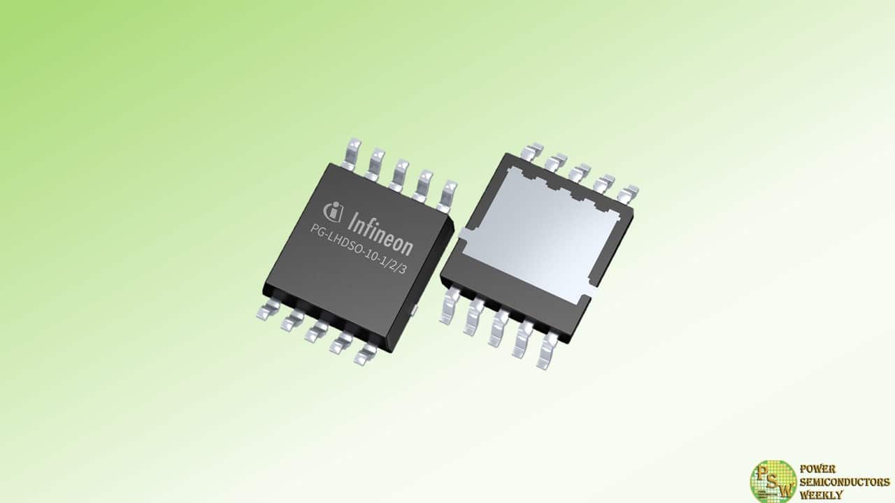
Infineon Technologies AG introduced the SSO10T TSC package with OptiMOS™ MOSFET technology. With its direct top-side cooling concept, the package offers excellent thermal performance. This eliminates heat transfer into or through the PCB of the automotive electronic control unit.
The package enables a simple and compact double-sided PCB design and minimizes cooling requirements and system costs for future automotive power designs. The SSO10T TSC is therefore well suited for applications such as electric power steering (EPS), EMB, power distribution, brushless DC drives (BLDC), safety switches, reverse battery, and DCDC converters.
The SSO10T TSC has a 5 x 7 mm² footprint and is based on the established industry standard SSO8, a 5 x 6 mm² robust housing. However, due to its top-side cooling, the SSO10 TSC offers more than 20 percent and up to 50 percent higher performance than the standard SSO8 – depending on the thermal interface (TIM) material used and the TIM thickness. The SSO10T TSC package is JEDEC listed for open market and provides wide second source compatibility. As a result, the package can be introduced quickly and easily as the future standard for top-side cooling.
The SSO10T package enables a very compact PCB design and reduces the system footprint. It also lowers the cost of the cooling design by eliminating vias, resulting in lower overall system costs and design effort. At the same time, the housing offers high power density and efficiency, thus supporting the development of future-proof and sustainable vehicles.
Original – Infineon Technologies
-

Alpha and Omega Semiconductor Limited announced its AONZ66412 XSPairFET™ MOSFET designed for Buck-Boost converters in USB PD 3.1 Extended Power Range (EPR) applications. The USB PD 3.1 EPR increases the USB-C maximum power up to 240W. AONZ66412 is defined to support the most commonly addressed power range of up to 140W at 28V, with two 40V N-Channel MOSFETs in a half-bridge configuration in a symmetric XSPairFET™ 5mmx6mm package.
The AONZ66412 can replace two single DFN5x6 MOSFETs, reducing the PCB area and simplifying the layout of the 4-switch buck-boost architecture while enabling a higher efficiency design. These benefits make the AONZ66412 ideal for buck-boost converters in Type-C USB 3.1 EPR applications, including notebook, USB hub, and power bank designs. The AONZ66412 is an extension to the AOS XSPairFET™ lineup that features the latest bottom source packaging technology and lower parasitic inductance for reduced switch node ringing.
Engineered with integrated high-side and low-side MOSFETs (3.8mOhms maximum on-resistance for each FET) within a DFN5x6 symmetric XSPairFET™ package, the low-side MOSFET source of the AONZ66412 is connected directly to a large paddle on the lead frame. This allows for improved thermals, as this paddle can be directly connected to the ground plane on the PCB. The improved package parasitics make 1MHz operation achievable, allowing inductor size and height to be reduced. AONZ66412 has been tested to achieve 97% efficiency @1MHz in typical USB PD 3.1 EPR conditions of 28V input, 17.6V output, and 8A load conditions.
“AOS specifically designed the AONZ66412 to meet EPR Type C PD application demands. AONZ66412 will reduce board space and improve power density to achieve the high-efficiency performance goals designers have set for this widely adopted USB-PD Type C application. AOS continues to be a leading innovator of buck-boost architecture solutions,” said Rack Tsai, Marketing Director of MOSFET product line at AOS.
Original – Alpha and Omega Semiconductor
-

Wolfspeed, Inc. hosted Senator Thom Tillis (R-NC) and other local officials, community partners, and employees at a ceremony to celebrate the topping out of construction at the $5 billion John Palmour Manufacturing Center for Silicon Carbide. Located in Chatham County, North Carolina, the JP will produce 200mm silicon carbide wafers, significantly expanding Wolfspeed’s materials capacity, and meet the demand for next generation semiconductors critical to the energy transition and AI.
“We are excited to mark this critical milestone alongside our hard-working team, loyal customers, community partners, and ardent supporters like Senator Thom Tillis,” said Wolfspeed President and CEO, Gregg Lowe.
“This facility is a testament to Wolfspeed’s commitment to our local community and domestic workforce, furthering our position as the global leader in silicon carbide production. The JP will help maintain America’s lead in energy innovation, and unlock significant benefits for our local community by growing the state’s economy by more than $17.5 billion over the next two decades and creating 1,800 good-paying jobs by 2030.”
“Wolfspeed’s $5 billion investment in Chatham County is another example of why North Carolina is the best state in the country to do business,” said Senator Tillis. “I was proud to vote in favor of the CHIPS and Science Act, which provides critical support for domestic semiconductor manufacturing, and I applaud Wolfspeed’s commitment to developing technology here in North Carolina that supports our national security and economic interests.”
The JP represents a total investment of $5 billion, complemented by public and private support, to help accelerate the transition from silicon to silicon carbide and ramp up supply of this material recently deemed as critical to the energy transition by the U.S. Department of Energy. By the end of 2024, phase one of construction is expected to be completed on the 445-acre site.
The ramp of the JP will support recently signed customer agreements with Renesas, Infineon, and additional companies, while driving meaningful progress towards Wolfspeed’s long-term growth strategy. The JP will primarily produce 200mm silicon carbide wafers, which are 1.7x larger than 150mm wafers, translating to more efficient wafers and ultimately, lower costs. The JP underpins Wolfspeed’s vision of accelerating the adoption of silicon carbide semiconductors across a wide array of end-markets and unlocking a new era of energy efficiency.
Wolfspeed currently produces more than 60% of the world’s silicon carbide materials at its Durham, N.C. headquarters, and is engaged in a $6.5 billion capacity expansion effort to dramatically increase production.
Original – Wolfspeed
