-

STMicroelectronics’ MasterGaN1L and MasterGaN4L introduce the next generation of integrated gallium-nitride (GaN) bridge devices that simplify power-supply design leveraging wide-bandgap technology to achieve the latest ecodesign targets.
ST’s MasterGaN family combines 650V GaN high electron-mobility transistors (HEMT) with optimized gate drivers, system protection, and an integrated bootstrap diode that helps power the device at startup. Integrating these features saves designers tackling the complex gate-drive requirements of GaN transistors. Housed in a compact power package, the devices also enhance reliability, cut the bill of materials, and ease circuit layout.
The latest devices contain two GaN HEMTs connected in half-bridge configuration. The arrangement is suitable for building switched-mode power supplies, adapters, and chargers with active-clamp flyback, active-clamp forward, and resonant converter topologies.
The MasterGaN1L and MasterGaN4L are pin compatible with MasterGaN1 and MasterGaN4 respectively. Compared to the earlier devices, they have a newly optimized turn-on delay that allows working at higher frequency and higher efficiency with low load, especially in resonant topologies.
The inputs accept signal voltages from 3.3V to 15V, with hysteresis and pull-down that facilitate connecting directly to a controlling device such as a microcontroller, DSP, or Hall-effect sensors. A dedicated shutdown pin helps designers save system power and the two GaN HEMTs have accurately matched timing with an interlocking circuit to prevent cross-conduction conditions.
The MasterGaN1L HEMTs have 150mΩ RDS(on) and 10A rated current, for use in applications up to 500W. Consuming just 20mW no-load power, and enabling high conversion efficiency, they enable designers to meet stringent industry targets for standby power and average efficiency. The MasterGaN4L HEMTs target applications up to 200W, with 225mΩ RDS(on) and rated current of 6.5A.
The EVLMG1LPBRDR1 and EVLMG4LPWRBR1 demonstration boards are available to help evaluate the features of each device. These boards contain a GaN-based half-bridge power module fine-tuned to work in an LLC application. They help quickly create new topologies leveraging the MasterGaN1L and MasterGaN4L devices without needing a complete PCB design.
Original – STMicroelectronics
-
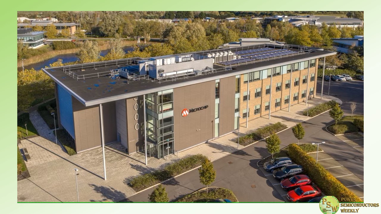
With UK and European companies seeking advanced technology to solve challenges in communications, IoT and automotive applications, many are looking for local support from major solution vendors. Microchip Technology Inc. announced the inauguration of a major new facility at Cambridge Research Park, Cambridge, UK.
At the heart of Microchip’s plans to develop more of its smart, connected and secure solutions in the UK area, the new center will add significant R&D space, which will allow Microchip’s business units to further develop their already broad offering. The new site will help Microchip improve its focus on the needs of several of its highest priority markets, such as IoT, automotive, industrial and consumer.
To gain immediate benefit from the facility, many of Microchip’s highly skilled development engineers and other staff will transfer from the company’s Ely site, with plans in hand to boost the number of employees at the Cambridge site over time.
“The Cambridge site is ideally situated in one the world’s top technology areas and will enable us to attract top talent to build state of the art products and serve our customer base,” said Sumit Mitra, senior corporate vice president of Microchip’s 32-bit microcontroller, microprocessor, wireless, aerospace and development tools business units.
“We have already onboarded a large number of talented and experienced engineers for the new center and expect that the new opportunities we will offer—to develop exciting solutions for the most significant and dynamic technology markets—will further attract the highly talented staff we need.”
“The facility is intended to become a premier Microchip engineering center, employing 200 highly skilled silicon engineering staff and advanced laboratories,” said Neel Das, senior director of Microchip’s 32-bit microcontroller business unit. “Establishing the new facility in Cambridge means we can meet this target by tapping into the wealth of engineering talent that exists in the area. The Cambridge Research Park is a hub of innovation and an excellent venue to develop the high-tech solutions on which we have built our reputation.”
The three-story building will offer approximately 10,000 square feet per floor, providing space to support multiple product lines including 16- and 32-bit microcontrollers, 32-bit microprocessors and wireless connectivity products plus technology development, physical design and human resource support.
Original – Microchip Technology
-

MACOM Technology Solutions Holdings, Inc. announced the completion of its acquisition of the radio frequency business of Wolfspeed, Inc. on December 2, 2023. The RF Business is highly complementary to MACOM’s portfolio and creates a compelling combined technology solution.
“We are excited to welcome the RF Business team to MACOM,” said Stephen G. Daly, President, Chief Executive Officer and Chair. “Going forward, we are committed to supporting all product and foundry customers and building upon the RF Business’ established technology to strengthen our leadership position.”
Original – MACOM Technology Solutions
-

DENSO Corporation announced changes to its organizational structure, executives’ responsibilities and personnel, effective January 1, 2024.
DENSO has stated at “DENSO DIALOG DAY 2023” that it will evolve from being “a Tier 1 supplier that supports the auto industry” to “a Tier 1 supplier that supports a mobility-centered society”, aiming to maximize the value of the entire mobility society, in addition to vehicles.
To achieve this, DENSO has announced its commitment to three challenges: “evolution of mobility,” “strengthening of foundational technology,” and “creating new value.” To materialize these goals, the following organizational and executive changes will be implemented.
In terms of the executive structure, two executive vice presidents will assume responsibility for the company’s major management resources in the following two areas, accelerating the formulation and execution of growth strategies. Additionally, to strengthen and expand technological development areas that will spur new growth, a Chief Innovation Officer (CIO) position will be established.
Original – DENSO
-

Axcelis Technologies, Inc. announced the grand opening of the Company’s new Axcelis Logistics Center, located at 105 Sam Fonzo Drive, Beverly, MA. The Company celebrated this milestone event with a ribbon-cutting ceremony led by President and CEO Russell Low.
The new Axcelis Logistics Center is a state-of-the-art facility designed to optimize Axcelis’ logistics and warehouse operations and provide flex capacity for the Company’s manufacturing operations to support the Company’s growth. The facility, which measures 101,800 square feet, was designed from the ground up to incorporate the latest technologies such as AI-driven autonomous mobile robots (AMRs) and other innovative enterprise-level warehouse automation to provide significant efficiency and improve material handling and flow to the Company’s operations.
The new center is designed to be energy efficient and employee friendly. It features EV charging stations, utilizes US EPA Energy Star rated heating, ventilation and air conditioning equipment and has all LED lighting with advanced motion sensors.
President and CEO Russell Low, commented, “The ribbon cutting represents the culmination of a vision ready to be set in full motion. Our investment in this new facility will allow us to support the Company’s expanding global customer base. We will continue to invest in our employees and infrastructure to ensure we have the necessary skills and capacity required to achieve our $1.3B financial model. We are also excited to provide significant employment opportunities across a wide variety of functions here in Beverly and across the globe. We look forward to continuing to play a vibrant role in our local communities and supply chain.”
The Company plans to seek a 25% tax credit under the U.S. Chips and Science Act relating to its capital investment in the new facility. The CHIPS and Science Act aims to bolster U.S. chip manufacturing to make American semiconductor supply chains more resilient and support national security and access to key technologies.
Original – Axcelis Technologies
