-
 LATEST NEWS / PRODUCT & TECHNOLOGY / SiC / TOP STORIES / WBG
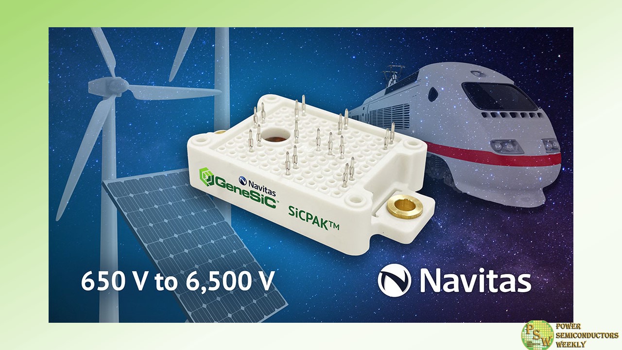
Navitas Launches into High-Power Markets with GeneSiC SiCPAK™ Modules and Accelerates Bare-Die Sales
May 8, 2023
2 Min ReadNavitas Semiconductor, the only pure-play, next-generation power semiconductor company, announced their expanded portfolio into higher power markets with their leading-edge silicon carbide (SiC) power products in SiCPAK™ modules and bare die.
Target applications cover centralized and string solar inverters, energy storage systems (ESS), industrial motion, electric vehicle (EV) on-board chargers, EV roadside fast chargers, wind energy, UPS, bi-directional microgrids, DC-DC converters, and solid-state circuit breakers.
Ranging from 650 V to 6,500 V, Navitas has the widest range of SiC technology. From an original line-up of discrete packages – from 8×8 mm surface-mount QFNs to through-hole TO-247s – the GeneSiC SiCPAK is an initial, direct entry point into higher-power applications. A comprehensive power-module roadmap, with high-voltage SiC MOSFETs and MPS diodes, GaN power ICs, high-speed digital isolators and low-voltage silicon control ICs is being mapped out.
Dr. Ranbir Singh, Navitas EVP for SiC noted, “With a complete portfolio of leading-edge power, control and isolation technology, Navitas will enable customers to accelerate the transition from fossil fuels, and legacy silicon power products to new, renewable energy sources and next-generation semiconductors, with more powerful, more efficient, faster-charging systems.”
SiCPAK™ modules employ ‘press-fit’ technology to offer compact form factors for power circuits and deliver cost-effective, power-dense solutions to end users. The modules are built upon GeneSiC die that have already made a mark in terms of superior performance, reliability, and ruggedness. Examples include a SiCPAK half-bridge module, rated at 6 mOhm, 1,200 V with industry-leading trench-assisted planar-gate SiC MOSFET technology. Multiple configurations of SiC MOSFETs and MPS diodes will be available to create application-specific modules for superior system performance. The initial release will include 1,200 V-rated half-bridge modules in 6, 12, 20, and 30mOhm ratings.
Within the lead-free SiCPAK, each SiC chip is silver (Ag) sintered to the module’s substrate for superior cooling and reliability. The substrate itself is ‘direct-bonded copper’ (DBC) and manufactured using an active-metal brazing (AMB) technique on silicon-nitride (Si3N4) ceramics, ideal for power-cycling applications. This construction delivers excellent strength and flexibility, fracture resistance, and good thermal conductivity for cool, reliable, long-life operation.
For customers who prefer to make their own high-power modules, all GeneSiC MOSFET and MPS diodes are available in bare die format, with gold (Au) and aluminum (Al) top-side metalizations.
Original – Navitas Semiconductor
-
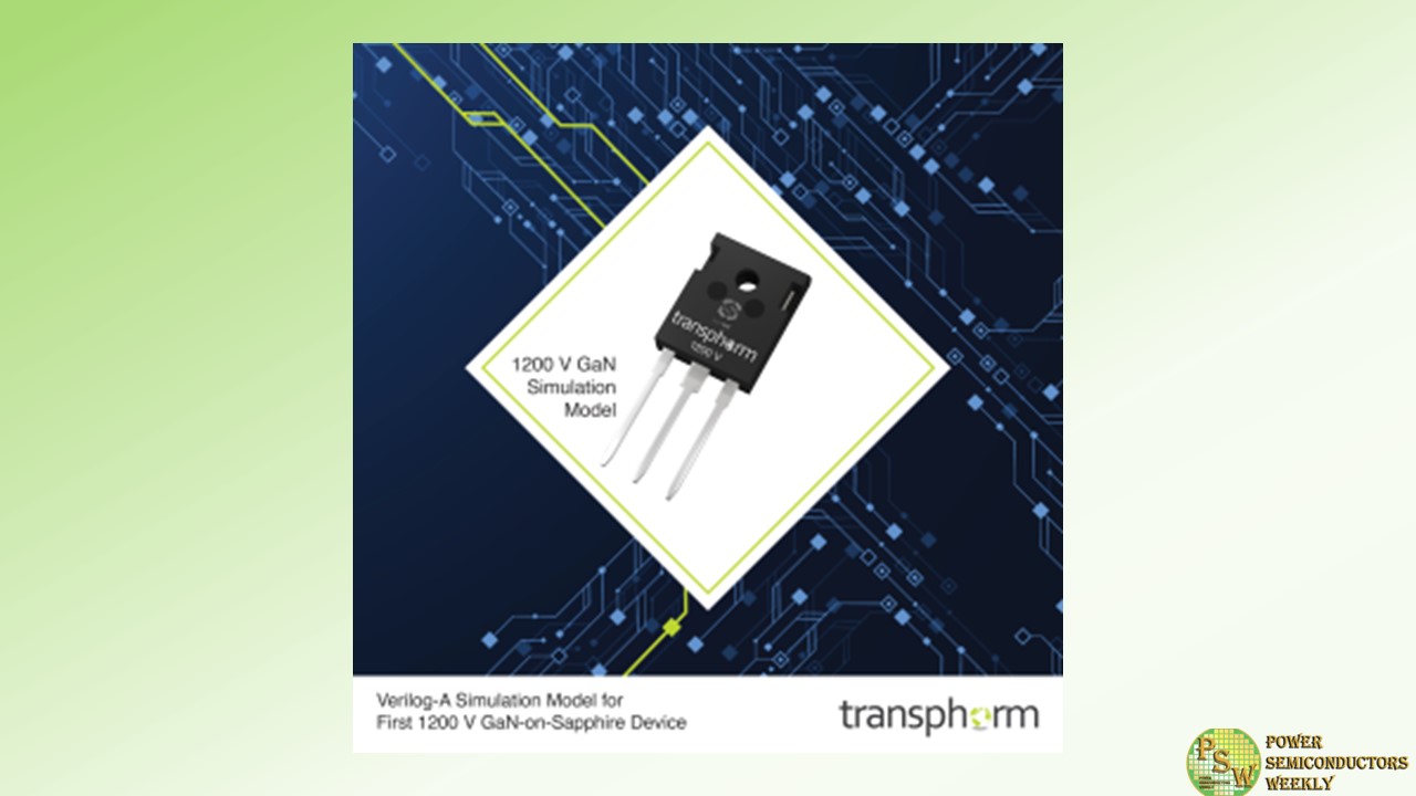
Transphorm, Inc. announced availability of its 1200 V FET simulation model and preliminary datasheet. The TP120H070WS FET is the only 1200 V GaN-on-Sapphire power semiconductor introduced to date, making its model the first of its kind. Its release indicates Transphorm’s ability to support future automotive power systems as well as three-phase power systems typically used in the broad industrial, datacom, and renewables markets. These applications will benefit from the 1200 V GaN device’s higher power density and reliability along with equal or better performance at more reasonable cost points versus alternative technologies.
Transphorm recently validated the GaN device’s higher performance ability in a 5 kW 900 V buck converter switching at 100 kHz. The 1200 V GaN device achieved 98.7% efficiency, exceeding that of a similarly rated production SiC MOSFET.
The innovative 1200 V technology also underscores Transphorm’s leadership in GaN power conversion. Vertical integration, epitaxy ownership, and patented process paired with decades of engineering expertise enable the company to bring to market the highest performing GaN device portfolio with four additional major differentiators: Manufacturability, Drivability, Designability, and Reliability.
Transphorm’s 1200 V technology is anchored in proven process and mature technology, satisfying customer confidence requirements. The GaN-on-Sapphire process is in volume production today in the LED market. Additionally, the 1200 V technology leverages the fundamentally superior, normally-off GaN platform used in Transphorm’s current device portfolio.
Key TP120H070WS device specifications include:
- 70 mΩ RDS(on)
- Normally off
- Efficient bidirectional current flow
- ± 20 Vmax gate robustness
- Low 4Vth gate drive noise immunity
- Zero QRR
- 3-lead TO-247 package
The Verilog-A device model is recommended for use with the SIMetrix Pro v8.5 Circuit Simulator. A LTSpice model is in development and will be released in Q4 2023. Simulation modeling allows for fast and efficient power system design validation while reducing design iterations, development time, and hardware investments.
The device model files and datasheet are available for download here: https://www.transphormusa.com/en/products/#models
1200 V FET samples are expected to be available by Q1 2024.
Original – Transphorm
