-
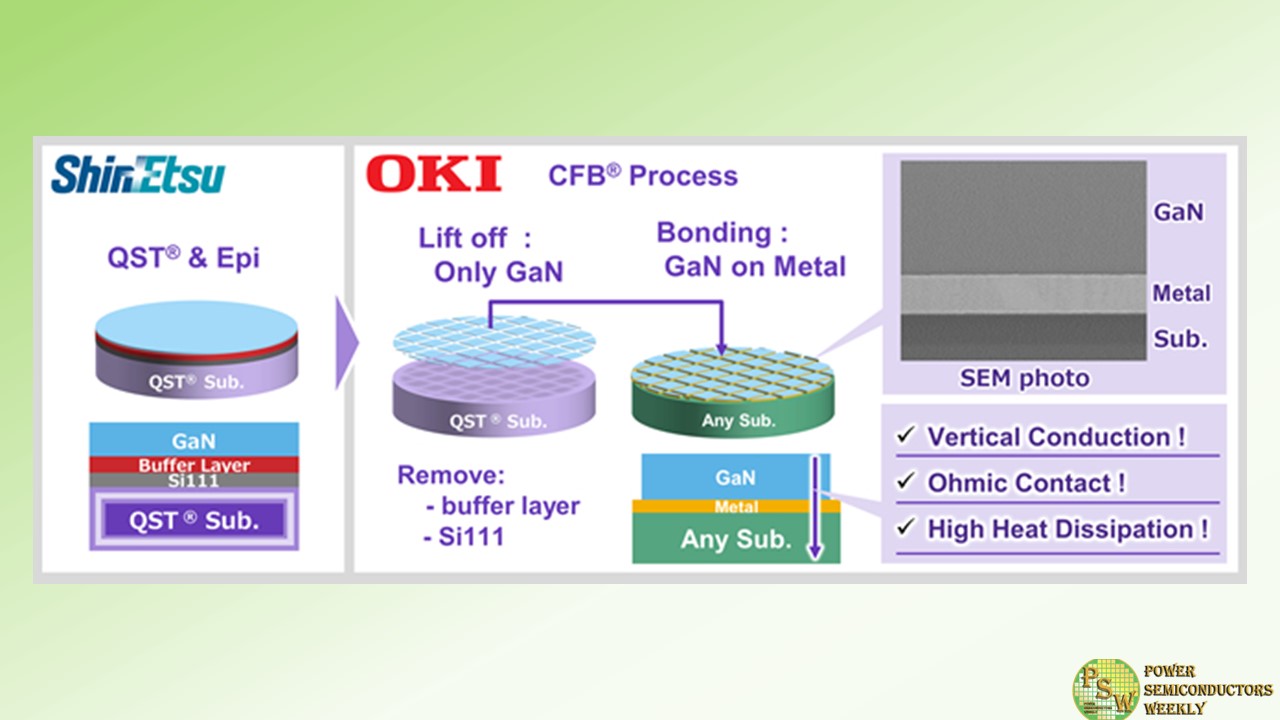
OKI, in collaboration with Shin-Etsu Chemical Co., Ltd., has announced the successful development of a technology that uses OKI’s CFB (crystal film bonding) technology to lift off only the GaN (gallium nitride) functional layer from Shin-Etsu Chemical’s uniquely improved QST® (Qromis Substrate Technology) substrate and bond it to a different material substrate.
This technology enables the vertical conduction of GaN and is expected to contribute to the realization and commercialization of vertical GaN power devices capable of controlling large currents. The two companies will work further together to develop vertical GaN power devices that can be implemented in society by partnering with companies that manufacture these devices.
GaN devices are attracting attention as next-generation devices that combine high device characteristics with low power consumption, such as power devices that require high breakdown voltages of 1800 volts or more, high-frequency devices for Beyond5G, and high-brightness micro-LED displays.
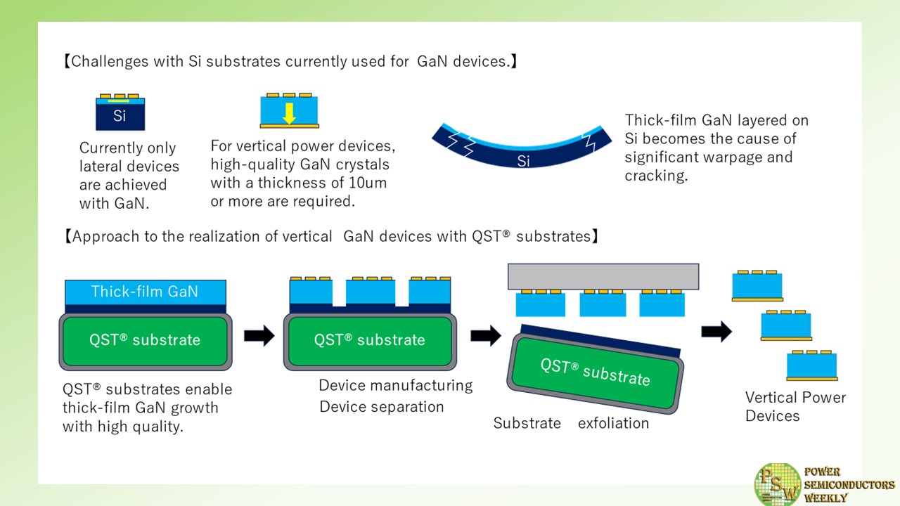
In particular, vertical GaN power devices are expected to achieve significant demand growth as devices that can improve the basic performance of electric vehicles by endowing them with extended driving ranges and shortened power supply times. However, two major challenges hinder the social implementation of vertical GaN power devices: the diameter of the wafers must be increased to improve productivity and vertical conductivity must be realized to enable large current control.
The coefficient of thermal expansion of Shin-Etsu Chemical’s QST substrate is equivalent to that of GaN. It can suppress warpage and cracking. This characteristic enables the crystal growth of thick GaN films with high breakdown voltages even on wafers larger than 8 inches, thereby enabling the production of wafers with larger diameters.
On the other hand, OKI’s CFB technology can lift off only the GaN functional layer from the QST substrate while maintaining high device characteristics. The insulating buffer layer required for GaN crystal growth can be removed and bonded to various substrates via metal electrodes that allow ohmic contact.
Bonding of these functional layers to a conductive substrate with high heat dissipation will enable both high heat dissipation and vertical conductivity. Through this, the combined technologies of Shin-Etsu Chemical and OKI solve the above two major challenges, paving the way for the social implementation of vertical GaN power devices.
In the future, the two companies will contribute to the realization and widespread use of vertical GaN power devices through Shin-Etsu Chemical’s provision of QST substrates or GaN grown QST substrates to companies manufacturing GaN devices and OKI’s provision of CFB technology through partnering and licensing.
Furthermore, OKI hopes to use CFB technology to provide added value to semiconductor devices that go beyond the framework of single materials and help realize the company’s key message of “Delivering OK! to your life”.
Original – OKI
-
Shin-Etsu Chemical Co., Ltd. has determined that QST® (Qromis Substrate Technology) substrate is an essential material for the social implementation of high-performance, energy-efficient GaN (gallium nitride) power devices, and the company will promote the development and launching on the market of these products.
Since QST® substrate is designed to have the same coefficient of thermal expansion (CTE) as GaN, it enables suppression of warpage and cracking of the GaN epitaxial layer and resultant large-diameter, high-quality thick GaN epitaxial growth. Taking advantage of these characteristics, it is expected to be applied to power devices and RF devices (5G and beyond 5G), which have been rapidly growing in recent years, as well as in such areas as MicroLED growth for MicroLED displays.
In addition to sales of QST® substrates, Shin-Etsu Chemical will also sell GaN grown QST® substrates upon customer request. We currently have a line-up of 6″ and 8″ diameter substrates, and we are working on 12″ diameter substrates. Since 2021, for each respective application for power devices, RF devices and LEDs, sample evaluation and device development are continuing with numerous customers in Japan and globally. Especially for power devices, continuous evaluation is underway for devices in the wide range of 650V to 1800V.
So far, Shin-Etsu Chemical has repeatedly made many improvements with regard to its QST® substrates. One example is the significant improvement in lowering defects originating from the bonding process, which has enabled the supply of high-quality QST® substrates. In addition, for the thicker GaN films that many of our customers have requested, we have promoted the provision of template substrates with optimized buffer layers, which enables our customers to realize stable epitaxial growth of more than 10 μm thickness. Furthermore, various successful results have been produced and reported on, including the achievement of thick-film GaN growth exceeding 20 μm using QST® substrates and the achievement of 1800V breakdown voltage in power devices.
Moreover, Shin-Etsu Chemical and Oki Electric Industry Co., Ltd. have jointly succeeded in developing a technology to exfoliate GaN from QST® substrates and bond it to substrates made of different materials using Crystal Film Bonding (CFB) technology. Until now, most GaN power devices have been lateral devices, but CFB technology takes advantage of the characteristics of QST® substrates to realize vertical power devices that can control large currents by exfoliating a thick layer of high-quality GaN from an insulating QST® substrate (see figure below).
To customers who manufacture GaN devices, Shin-Etsu Chemical will provide QST® substrates or GaN grown QST® substrates and Oki Electric Industry will provide its CFB technology through partnering or licensing. In this way, the two companies hope to contribute to the advancement of vertical power devices.
Based on these development results and also based on business situation inquiries from customers, Shin-Etsu Chemical will continue to increase production to meet customer demand.
Shin-Etsu Chemical will contribute to the realization of a sustainable society that can use energy efficiently by further promoting the social implementation of GaN devices that have characteristics that are absolutely essential for the future society.
Original – Shin-Etsu Chemical
