-
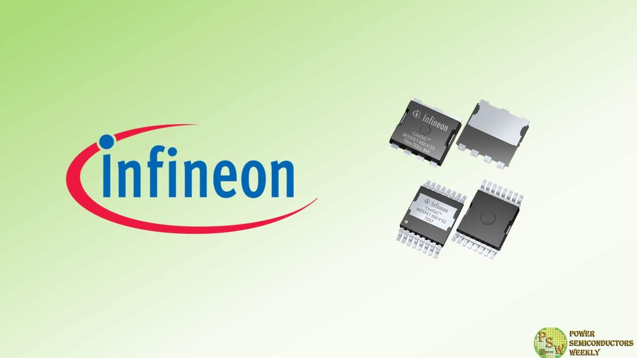
The electronics industry is witnessing a significant shift towards more compact and powerful systems, driven by technological advancements and a growing focus on decarbonization efforts. With the introduction of the Thin-TOLL 8×8 and TOLT packages, Infineon Technologies AG is actively accelerating and supporting these trends. They enable a maximum utilization of the PCB mainboard and daughter cards, while also taking the system’s thermal requirements and space restrictions into account.
The company is now expanding its portfolio of CoolSiC™ MOSFET discretes 650 V with two new product families housed in the Thin-TOLL 8×8 and TOLT packages. They are based on the CoolSiC Generation 2 (G2) technology, offering significantly improved figures-of-merit, reliability, and ease-of-use. Both product families specifically target high and medium switching-mode power supplies (SMPS), including AI servers, renewable energy, EV chargers, and large home appliances.
The Thin-TOLL package has a form factor of 8×8 mm and offers the best-in-class Thermal Cycling on Board (TCoB) capability on the market. The TOLT package is a top-side cooled (TSC) enclosure with a similar form factor to TOLL. Both package types offer developers several benefits: Using them in AI and server power supply units (PSU), for example, reduces the thickness and length of the daughter cards and allows for a flat heat sink.
When used in microinverters, 5G PSU, TV PSU and SMPS, the Thin-TOLL 8×8 package allows for a minimization of the PCB area occupied by the power supply devices on the mainboard, while TOLT keeps the junction temperature of the devices under control, given that these applications typically use convection cooling. In addition, TOLT devices complete Infineon’s top-side cooled CoolSiC industrial portfolio, namely CoolSiC 750 V in Q-DPAK. They enable developers to reduce the PCB footprint occupied by SiC MOSFETs when the power to be delivered to the devices does not require a Q-DPAK package.
The CoolSiC MOSFETs 650 V G2 in ThinTOLL 8×8 and TOLT are now available in R DS(on) from 20, 40, 50 and 60 mΩ. Additionally, the TOLT variant is also available with an R DS(on) of 15 mΩ. The product family will be expanded by a more granular portfolio by the end of 2024. More information is available at www.infineon.com/coolsic-gen2. Infineon will showcase the CoolSiC MOSFET 650 V Generation 2 at the PCIM in Nuremberg.
Original – Infineon Technologies
-

Infineon Technologies AG will provide silicon carbide (SiC) power modules HybridPACK™ Drive G2 CoolSiC™ and bare die products to Xiaomi EV for its recently announced SU7 until 2027. Infineon’s CoolSiC-based power modules allow for higher operating temperatures, resulting in best-in-class performance, driving dynamics and lifetime.
Traction inverters based on the technology can, for example, further increase electric vehicle range. The HybridPACK Drive is Infineon’s market-leading power module family for electric vehicles, with almost 8.5 million units sold since 2017.
Infineon provides two HybridPACK Drive G2 CoolSiC 1200 V modules for the Xiaomi SU7 Max. In addition, Infineon supplies Xiaomi EV with a broad range of products per car, including, for example, EiceDRIVER TM gate drivers and more than ten microcontrollers in various applications. The two companies also agreed to further cooperate on SiC automotive applications to fully utilize the benefits of Infineon’s SiC portfolio.
Zhenyu Huang, Vice President of Xiaomi EV and General Manager of the Supply Chain Department, said: “Infineon is an important partner with leading technologies and resilient manufacturing capabilities in power semiconductors as well as a highly scalable microcontroller product portfolio. The cooperation between the two companies will not only help stabilize the supply of silicon carbide for Xiaomi EV, but also help us build a high-performance, safe and reliable luxury car with leading-edge features for our customers.”
Peter Schiefer, President of Infineon’s Automotive division, said: “We are very pleased to work with dynamic players such as Xiaomi EV and provide them with silicon carbide products designed to enhance the performance of electric cars even further. As the leading partner to the automotive industry, we are well positioned with our broad product portfolio, system understanding and multi-site manufacturing base to shape the mobility of the future.”
This collaboration contributes to Infineon’s position as the number one partner of the global automotive industry. According to the latest data from TechInsights, Infineon is the largest semiconductor supplier to the automotive industry. In addition to its number one position in automotive power semiconductors, Infineon also took the lead in the field of automotive microcontrollers last year.
Original – Infineon Technologies
-
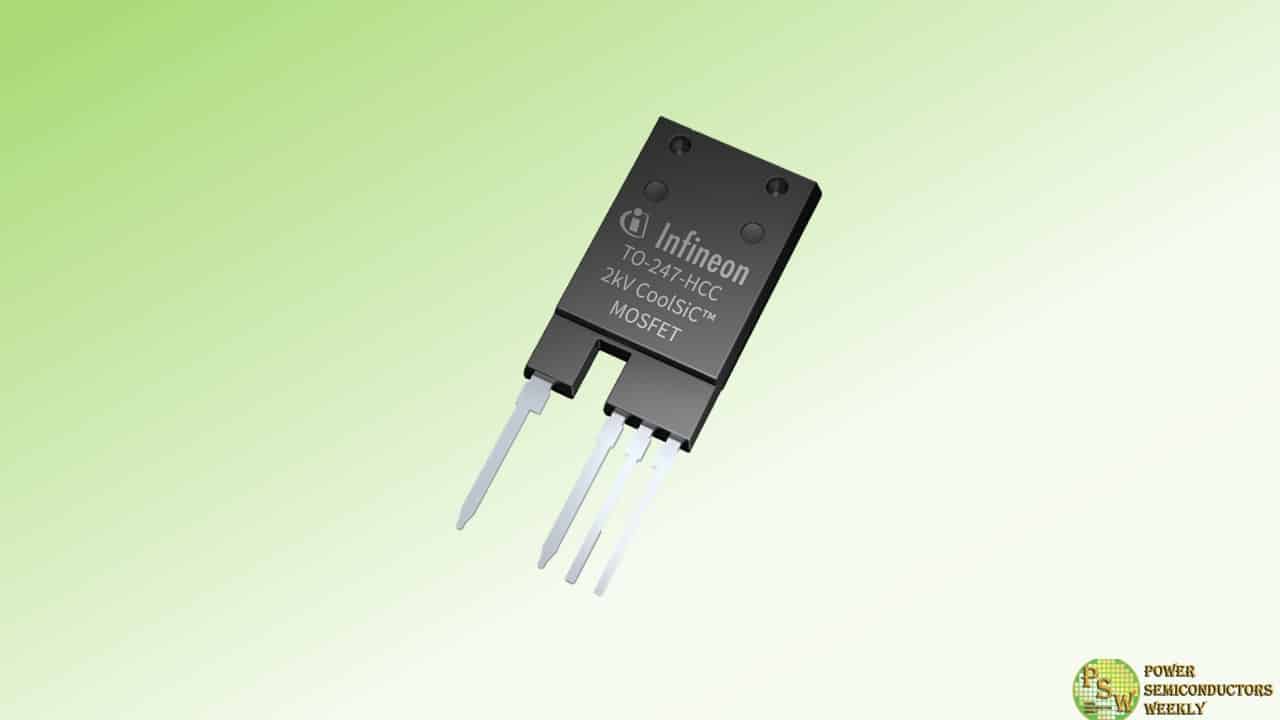
Infineon Technologies AG introduced the new CoolSiC™ MOSFETs 2000 V in the TO-247PLUS-4-HCC package to meet designers’ demand for increased power density without compromising the system’s reliability even under demanding high voltage and switching frequency conditions.
The CoolSiC MOSFETs offer a higher DC link voltage so that the power can be increased without increasing the current. It is the first discrete silicon carbide device with a breakdown voltage of 2000 V on the market and comes in a TO-247PLUS-4-HCC package with a creepage distance of 14 mm and clearance distance of 5.4 mm. With low switching losses, the devices are ideal for solar (e.g. string inverters) as well as energy storage systems and electric vehicle charging applications.
The CoolSiC MOSFET 2000 V product family is ideally suited for high DC link systems with up to 1500 V DC. Compared to 1700 V SiC MOSFETs, the devices also provide a sufficiently high overvoltage margin for 1500 V DC systems. The CoolSiC MOSFETs deliver a benchmark gate threshold voltage of 4.5 V and are equipped with a robust body diode for hard commutation. Due to the .XT connection technology, the components offer first-class thermal performance. They are also highly resistant to humidity.
In addition to the CoolSiC MOSFETs 2000 V, Infineon will soon be launching the matching CoolSiC diodes: The first launch will be the 2000 V diode portfolio in the TO-247PLUS 4-pin package in the third quarter of 2024, followed by the 2000 V CoolSiC diode portfolio in the TO-247-2 package in the final quarter of 2024. These diodes are particularly suitable for solar applications. A matching gate driver portfolio is also available.
The CoolSiC MOSFET 2000 V product family is available now. In addition, Infineon also offers a suitable evaluation board: the EVAL-COOLSIC-2KVHCC. Developers can use the board as a precise universal test platform to evaluate all CoolSiC MOSFETs and diodes 2000 V and the EiceDRIVER™ Compact Single Channel Isolated Gate Driver 1ED31xx product family through double pulse or continuous PWM operation.
Original – Infineon Technologies
-
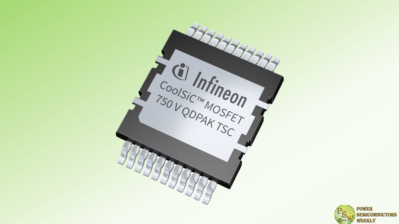
Infineon Technologies AG introduced the 750V G1 discrete CoolSiC™ MOSFET to meet the increasing demand for higher efficiency and power density in industrial and automotive power applications. The product family includes both industrial-graded and automotive-graded SiC MOSFETs that are optimized for totem-pole PFC, T-type, LLC/CLLC, dual active bridge (DAB), HERIC, buck/boost, and phase-shifted full bridge (PSFB) topologies.
The MOSFETs are ideal for use in both typical industrial applications, such as electric vehicle charging, industrial drives, solar and energy storage systems, solid state circuit breaker, UPS systems, servers/ datacenters, telecom, and in the automotive sector, such as onboard chargers (OBC), DC-DC converters, and many more.
The CoolSiC MOSFET 750 V G1 technology features excellent RDS (on) x Q fr and superior RDS (on) x Q oss Figure-of-Merits (FOMs), resulting in ultra-high efficiency in hard-switching and soft-switching topologies respectively. Its unique combination of high threshold voltage (V GS(th), Typ. of 4.3 V) with low Q GD/Q GS ratio ensures high robustness against parasitic turn-on and enables unipolar gate driving, leading to increased power density and low cost of the systems.
All devices use Infineon’s proprietary die-attach technology which delivers outstanding thermal impedance for equivalent die sizes. The highly reliable gate oxide design combined with Infineon’s qualification standards delivers robust and long-term performance.
With a granular portfolio ranging from 8 to 140 mΩ RDS (on) at 25°C, this new CoolSiC MOSFET 750 V G1 product family meets a wide range of needs. Its design ensures lower conduction and switching losses, boosting overall system efficiency.
Its innovative packages minimize thermal resistance, facilitate improved heat dissipation, and optimize in-circuit power loop inductance, thereby resulting in high power density and reduced system costs. It’s important to note that this product family features the cutting-edge QDPAK top-side cooled package.
Original – Infineon Technologies
-

Arrow Electronics, Inc. and its engineering services company, eInfochips, are working with Infineon Technologies AG to help eInfochips’ customers accelerate the development of electric vehicle (EV) chargers.
Development of EV chargers, especially DC “fast chargers,” is becoming increasingly challenging to equipment manufacturers due to several factors, such as lack of prior experience, stringent functional safety and reliability requirements, and a fledgling support network. The collaboration between Arrow and Infineon aims to help innovators navigate these challenges while accelerating time-to-market.
As part of the collaboration, Arrow’s High Power Center of Excellence has developed a 30kW DC fast charger reference platform. This includes Infineon’s 1200V CoolSiC™ Easy power modules and also hardware design, embedded firmware, bi-directional charging support and energy metering functionality.
“Combining Arrow’s strength in components, engineering and design services with Infineon’s innovative products will help customers accelerate their design and speed to market in e-mobility applications,” said Murdoch Fitzgerald, vice president, global engineering and design services at Arrow. “Customers can rely on this collaboration to deliver innovative and leading edge DC faster chargers, accelerate and de-risk design cycles, and get access to a world-class support team enabling them to plan and manage their product roadmap and lifecycles.”
“Infineon is on a drive towards decarbonization and digitalization with our ecosystem partners, and this collaboration with Arrow is a testament to this mission,” said Shri Joshi, vice president of Green Industrial Power, Infineon Technologies Americas. “The joint 30kW DC fast charger reference platform, which includes Infineon’s latest power modules and devices, will help our customers bring more fast chargers to market as the future moves to electrical vehicles. We look forward to this ongoing collaboration to support our customer base.”
The first reference design from this collaboration, a production-grade 30kW DC fast charger reference development platform, is being demonstrated at Applied Power Electronics Conference, Feb. 25-29, in Long Beach, Calif.
Original – Arrow Electronics
-
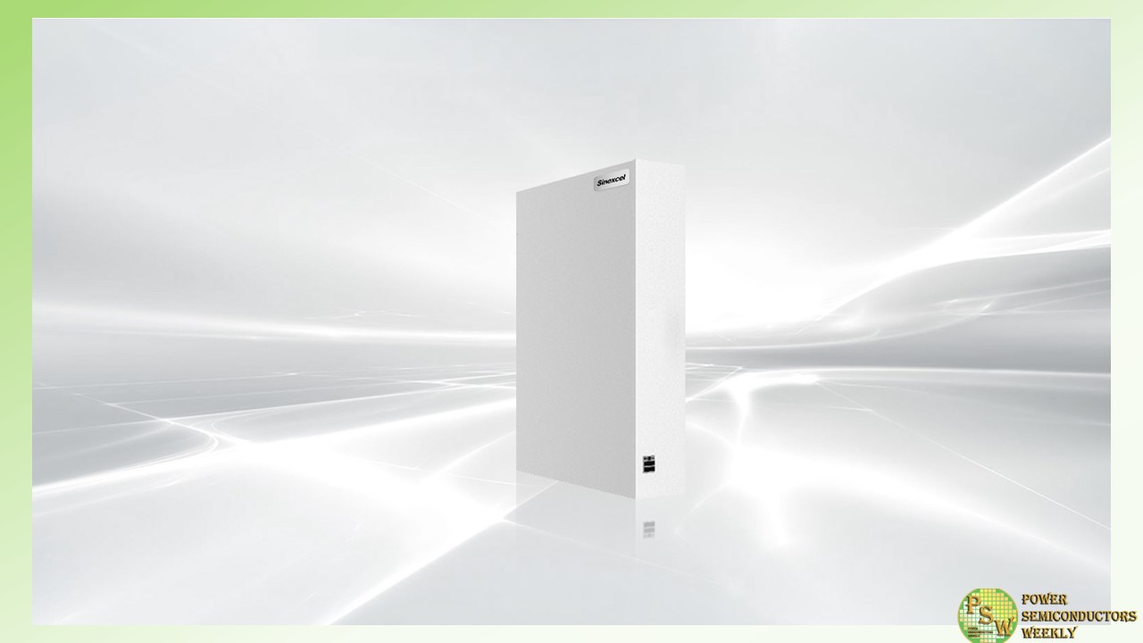
Infineon Technologies AG announced a partnership with Shenzhen based Sinexcel Electric Co., Ltd., a global leader in core power equipment and solutions for the Energy Internet. Infineon will provide Sinexcel with its industry-leading 1200 V CoolSiC™ MOSFET power semiconductor devices in combination with EiceDRIVER™ compact 1200 V single-channel isolated gate drive ICs to further improve the efficiency of energy storage systems.
Driven by the carbon peaking and carbon neutrality strategy and the new energy wave, the domestic energy storage market has maintained sustained and rapid development in recent years. According to the Chinese Ministry of Industry and Information Technology, in the first half of 2023, the newly installed capacity of energy storage reached 8.63 GWh, equivalent to the total installed capacity of previous years.
The efficiency and power density of energy storage systems are important factors of product competitiveness, while the size, weight and cost of energy storage systems are closely related to the energy conversion efficiency and directly affect the product cost. Therefore, power semiconductor components play a crucial role.
“The SiC power solution is an important component for future green energy production and storage applications. Infineon’s cooperation with Sinexcel in the field of energy storage inverters enables energy storage systems to achieve advantages such as high efficiency, small size, and light weight, providing a solid guarantee for high-reliability and high-performance energy storage systems,” said Mr. Yu Daihui, Senior Vice President of Infineon Technologies and Head of Green Industrial Power Division in Greater China.
“By using Infineon’s SiC devices, Sinexcel’s energy storage products are obviously more compact and flexible, with significantly higher efficiency and lower losses, which reduces the heat dissipation cost of systems, is conducive to the long-term efficient and stable operation of products, and helps end users improve their operational stability and shorten their return on investment cycle.
This greatly improves the system competitiveness of our products and enhances the trust of clients in our energy storage products and the brand awareness of Sinexcel. We hope that in the future, Infineon will further provide high-performance and high-stability components to help enhance the competitiveness of Sinexcel’s products on the client side,” said Mr.Wei Xiaoliang, Deputy General Manager of Sinexcel.
With more than 20 years of product development and application experience in the SiC field, Infineon has been working nonstop to develop more sophisticated SiC products. Due to their high power density, Infineon’s 1200 V CoolSiC MOSFETs can reduce losses by 50 percent and provide ~2 percent additional energy without increasing the battery size, which is especially beneficial for high-performance, lightweight and compact energy storage solutions.
By using Infineon’s 1200 V CoolSiC MOSFETs and EiceDRIVER compact 1200 V single-channel isolated gate drive ICs, Sinexcel’s energy storage converters achieve high power density, minimum electromagnetic radiation and interference, high protection performance and high reliability. This allows a system efficiency of up to 98 percent, which is 1 percent higher than that of traditional solutions, reaching the industry-leading level and better meeting the needs of on-grid and off-grid energy storage applications in both domestic and overseas markets.
Original – Infineon Technologies
-
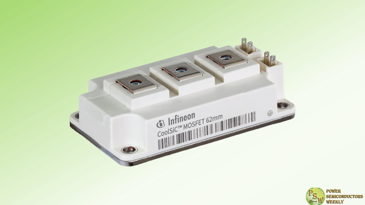
Infineon Technologies AG announced the expansion of its CoolSiC 1200 V and 2000 V MOSFET module families with a new industry-standard package. The proven 62mm device is designed in half-bridge topology and is based on the recently introduced and advanced M1H silicon carbide (SiC) MOSFET technology.
The package enables the use of SiC for mid-power applications from 250 kW – where silicon reaches the limits of power density with IGBT technology. Compared to a 62mm IGBT module, the list of applications now additionally includes solar, server, energy storage, EV charger, traction, commercial induction cooking and power conversion systems.
The M1H technology enables a significantly wider gate voltage window, ensuring high robustness to driver and layout-induced voltage spikes at the gate without any restrictions even at high switching frequencies. In addition to that, very low switching and transmission losses minimize cooling requirements.
Combined with a high reverse voltage, these devices meet another requirement of modern system design. By using Infineon’s CoolSiC chip technology, converter designs can be made more efficient, the nominal power per inverter can be increased and system costs can be reduced.
With baseplate and screw connections, the package features a very rugged mechanical design optimized for highest system availability, minimum service costs and downtime losses. Outstanding reliability is achieved through high thermal cycling capability and a continuous operating temperature (T vjop) of 150°C. The symmetrical internal package design provides identical switching conditions for the upper and lower switches. Optionally, the thermal performance of the module can be further enhanced with pre-applied thermal interface material (TIM).
The CoolSiC 62mm package MOSFETs are available in 1200 V variants of 5 mΩ/180 A, 2 mΩ/420 A and 1 mΩ/560 A. The 2000 V portfolio will include the 4 mΩ/300 A and 3 mΩ/400 A variants. The portfolio will be completed in Q1 2024 with the 1200 V/3 mΩ and 2000 V/5 mΩ variants.
An evaluation board is available for rapid characterization of the modules (double pulse/continuous operation). For ease of use, it provides flexible adjustment of the gate voltage and gate resistors. At the same time, it can be used as a reference design for driver boards for volume production.
Original – Infineon Technologies
-
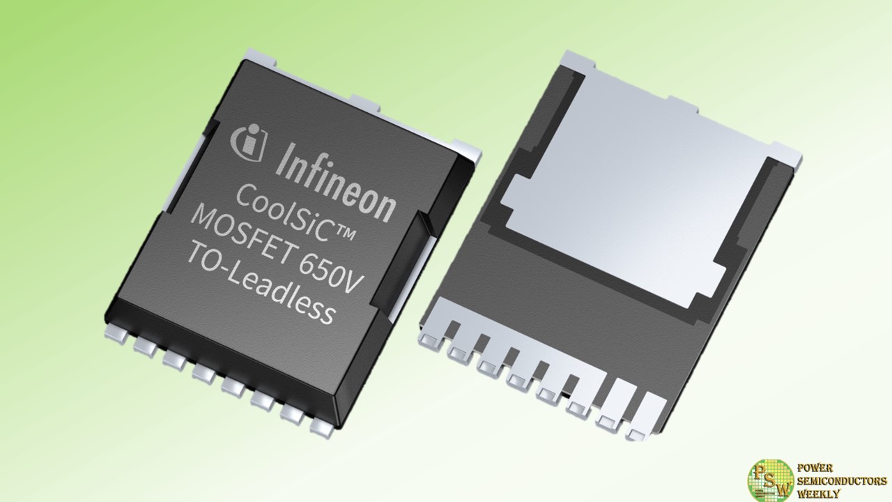
As digitalization, urbanization, and the rise of electro-mobility continue to shape the rapidly evolving world, the demand for power consumption is reaching unprecedented levels. Acknowledging energy efficiency as an important concern, Infineon Technologies AG addresses these megatrends with its silicon carbide (SiC) CoolSiC™ MOSFET 650 V in TO leadless (TOLL) packaging. The new SiC MOSFETs are enhancing Infineon’s comprehensive CoolSiC portfolio and are optimized for the lowest losses, the highest reliability, and ease-of-use in applications such as SMPS for servers, telecom infrastructure as well as energy storage systems and battery formation solutions.
The CoolSiC 650 V high-performance trench-based power SiC MOSFETs are offered in a very granular portfolio to best suit different target applications. The new family comes in a JEDEC-qualified TOLL package featuring a low parasitic inductance, allowing for higher switching frequency, reduced switching losses, good thermal management, and automated assembly. The compact form factor enables efficient and effective usage of the board space, empowering system designers to achieve exceptional power density.
The CoolSiC MOSFETs 650 V showcase remarkable reliability even in harsh environments, making them an ideal choice for topologies with repetitive hard commutation. The inclusion of the innovative .XT interconnect technology further enhances the devices’ thermal performance by reducing the thermal resistance (R th) and thermal impedance (Z th). In addition, the new devices feature a gate threshold voltage (V GS(th)) greater than 4 V for robustness against parasitic turn-on, a robust body diode, and the strongest gate oxide (GOX) in the market resulting in extremely low FIT (failures in time) rates.
While a cut-off voltage (V GS(off)) of 0 V is generally recommended to simplify the driving circuit (unipolar driving), the new portfolio supports a wide driving interval of V GS voltage within the range of -5 V (turn-off) to 23 V (turn-on). This ensures ease-of-use and compatibility with other SiC MOSFETs and standard MOSFET gate-driver ICs. This is paired with higher reliability, reduced system complexity, and the enablement of automated assembly, reducing system and production costs and accelerating time-to-market.
Original – Infineon Technologies
