-
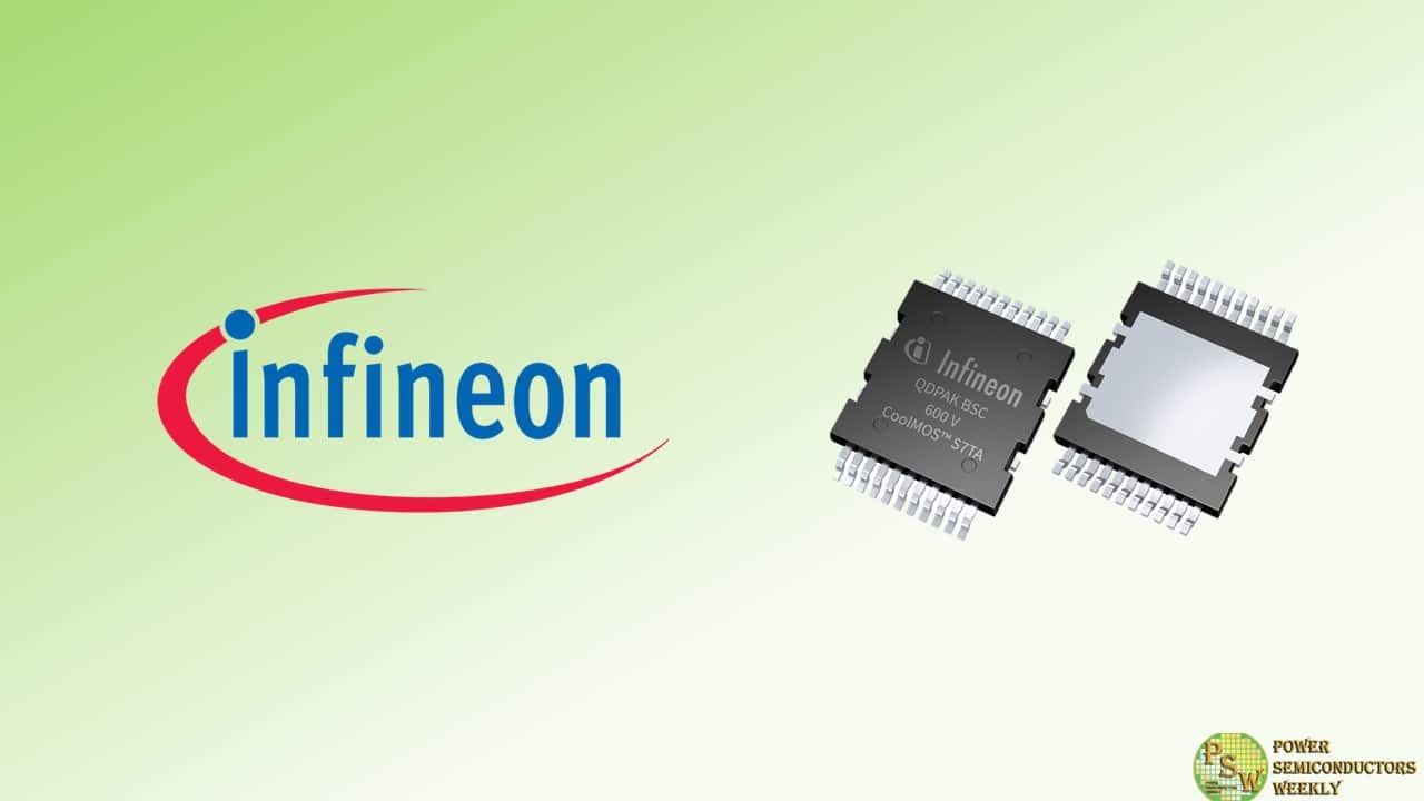
Infineon Technologies AG introduced the 600 V CoolMOS™ S7TA Superjunction MOSFET for automotive power management applications. Designed to meet the specific requirements of automotive electronics, the S7TA features an integrated temperature sensor that significantly improves the accuracy of junction temperature sensing, building on the advances made by its counterpart for industrial applications (CoolMOS S7T). The resulting benefits include improved durability, safety, and efficiency, all of which are essential in the automotive domain.
Like its industrial counterpart, the automotive-graded CoolMOS S7TA is particularly well suited for solid-state relay (SSR) applications, demonstrating superior R DS(on) and sensing accuracy, which is crucial for various automotive electronic devices that rely on efficient power management solutions. The integration of a Superjunction MOSFET with an embedded temperature sensor in the same package enhances the performance of SSRs and ensures dependable operation even under the most severe overload conditions, which is an absolute necessity for automotive applications where reliability is non-negotiable.
The embedded sensor of the S7TA offers a 40 percent increase in accuracy and up to four times faster response time than standalone on-board sensors. Such advances in temperature monitoring are critical for automotive applications, enabling individual monitoring within multi-device systems, thereby improving reliability, and preventing thermal issues that can lead to system failures.
The optimized power transistor utilization of the CoolMOS S7TA promises not only superior performance, but also precise control of the output stage. This level of precision is key to reducing power consumption and energy costs, which is a pressing concern in automotive applications where efficiency translates directly into vehicle range and operational economy. Compared to traditional electromechanical relays, the CoolMOS S7TA offers a significant improvement in total power dissipation.
The CoolMOS S7TA further provides a high overcurrent threshold, which serves to increase the reliability of the SSR and reduce the likelihood of failures. The robust switching solution paves the way for safer operations within the vehicle, and the enhanced robustness of the MOSFETs leads to a longer automotive relay lifecycle, resulting in lower maintenance and replacement costs.
The 600 V CoolMOS S7TA provides an optimized solution for potential applications that are central to the safety and functionality of modern vehicles. These include critical components such as circuit breakers, encompassing high-voltage battery disconnect switches, low-frequency switches for both direct current (DC) and alternating current (AC), as well as high-voltage electronic fuses (HV eFuses).
Infineon also introduces the EVAL_eFuse_PoC_400V_S7, a proof-of-concept board that showcases the robustness and versatility of an automotive eFuse. The board demonstrates a reliable method for safeguarding automotive electrical systems, featuring an interchangeable power stage that adapts to various operating conditions with different voltage classes and cooling methods.
Both the 600 V CoolMOS S7T in automotive and industrial grades are already available and come in QDPAK TSC and BSC packages, offering a range of R DS(on) from 17 to 40 mΩ. The 10 mΩ variant will be added to the lineup in the second half of 2024. Further information is available at www.infineon.com/s7ta and www.infineon.com/s7t.
Original – Infineon Technologies
-
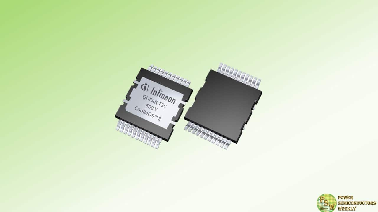
Infineon Technologies AG introduced the 600 V CoolMOS™ 8 high voltage superjunction (SJ) MOSFET product family. The devices combine the best features of the 600 V CoolMOS 7 MOSFET series and are the successors to the P7, PFD7, C7, CFD7, G7 and S7 product families. The new superjunction MOSFETs enable cost-effective Si-based solutions that enhance Infineon’s wide-bandgap offering. They are equipped with an integrated fast body diode, making them suitable for a wide range of applications such as server and industrial switched-mode power supply units (SMPS), EV chargers, and micro-solar.
The components come in SMD QDPAK, TOLL and ThinTOLL 8 x 8 packages, which simplifies designs and reduces assembly costs. At 10 V, the 600 V CoolMOS 8 SJ MOSFETs offer 18 percent lower gate charge (Q g) than the CFD7 and 33 percent lower than the P7. At 400 V, the product family offers a 50 percent lower output capacitance C OSS than the CFD7 and the P7.
In addition, the turn-off losses (E oss) have been reduced by 12 percent compared to the CFD7 and the P7 and the reverse recovery charge (Q rr) is 3 percent lower compared to the CFD7. Furthermore, the devices offer the lowest reverse recovery time (t rr) on the market and the thermal performance has been improved by 14 to 42 percent compared to the previous generation.
With these features, the devices offer high efficiency and reliability in soft-switching topologies such as LLC and ZVS phase-shift full-bridge. They also provide excellent performance levels in PFC, TTF and other hard-switching topologies. Due to their optimized R DS(on), the devices offer higher power density, allowing products in a Si-based super junction (SJ) technology to be reduced to a single-digit value of 7 mΩ.
Infineon will showcase the 600 V CoolMOS 8 SJ MOSFETs at the Infineon booth (Hall 7 / Booth 470) at PCIM 2024 in Nuremberg. Samples of the 600 V CoolMOS 8 SJ MOSFETs are now available. More information is at www.infineon.com/coolmos8.
Original – Infineon Technologies
-
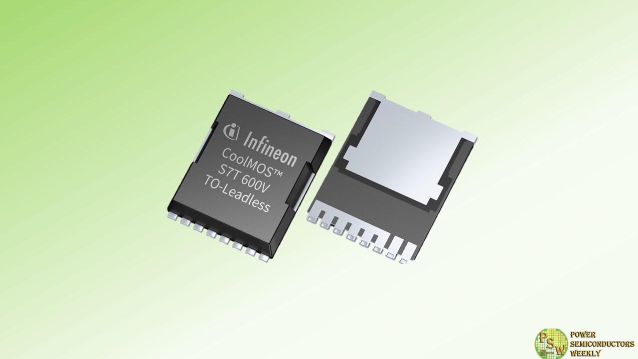
Infineon Technologies AG launches its new CoolMOS™ S7T product family with an integrated temperature sensor to improve the accuracy of junction temperature sensing. The integration of these products has a positive impact on the durability, safety, and efficiency of many electronic applications. The CoolMOS S7T is best suited for solid-state relay (SSR) applications for enhanced performance and reliability due to its superior R DS(on) and the highly accurate, embedded sensor.
Since SSRs are fundamental components in various electronic devices, customers can benefit in many ways from a superjunction MOSFET with an integrated sensor in the same package. Infineon’s innovative approach improves the relay’s performance and ensures reliable operation even under overload conditions. The integrated temperature sensor provides up to 40 percent greater accuracy and ten times faster response time than a standard independent on-board sensor located at the drain. Additionally, the monitoring process can be performed individually within a multi-device system for improved reliability.
The CoolMOS S7T enables optimal utilization of the power transistor, resulting in enhanced performance and precise control of the output stage. Compared to electromechanical relays, the total power dissipation can be improved up to two times, while current solid state triac solutions are more than 5 times less efficient. Improved efficiency and the ability to handle higher loads help in reducing power consumption and energy costs.
Unique output stage performance, coupled with a significant overcurrent threshold, bolster relay reliability and minimizes the risk of failure and downtime. The rugged switching solution also ensures safer operation. As a result of the MOSFETs increased robustness, the life of the relay is improved, leading to less frequent replacement. Ultimately, all of these benefits translate into lower maintenance costs.
Original – Infineon Technologies
-

The accelerated transition to electric vehicles has led to significant innovations in charging systems that demand more cost-efficient and high performing power electronics. Addressing this, Infineon Technologies AG expands its 650 V CoolMOS™ CFD7A portfolio by introducing the QDPAK package.
This package family is designed to provide equivalent thermal capabilities with improved electrical performance over the well-known TO247 THD devices, thus enabling efficient energy utilization in onboard chargers and DC-DC converters.
Efficient and powerful electric vehicle charging systems help reduce charging times and vehicle weight, increasing design flexibility and reduce the total cost of ownership of the vehicle. This new addition complements the existing CoolMOS CFD7A series, offering versatility with top-side and bottom-side cooled packages. The QDPAK TSC (top side cooled), enables designers to achieve higher power densities and optimal PCB space utilization.
The 650 V CoolMOS CFD7A offers several important features for reliable operation in high-voltage applications. Thanks to its reduced parasitic source inductance, the device can minimize electromagnetic interference (EMI), ensuring clear signals and consistent performance.
The Kelvin source pin also provides improved precision for current sensing, ensuring accurate measurements even in challenging conditions. With a creepage distance suitable for high voltage applications, as well as high current capability and high power dissipation (P tot) of up to 694 W at 25°C, it is a versatile and powerful device for a wide range of high-voltage applications.
New system designs using 650 V CoolMOS CFD7A in QDPAK TSC will maximize PCB space use, doubling power density and enhancing thermal management via substrate thermal decoupling. This approach simplifies assembly, eliminates board stacking and reduces the need for connectors, thereby lowering system costs. The power switch reduces thermal resistance by up to 35 percent, providing high power dissipation that outperforms standard cooling solutions.
This feature overcomes the thermal limitations of bottom side cooled SMD designs using FR4 PCBs, resulting in a significant boost in system performance. The optimized power loop design locates drivers near the power switch, improving reliability by reducing stray inductance and chip temperatures. Overall, these features contribute to a cost-effective, robust, and efficient system ideal for modern power needs.
As announced in February 2023, the QDPAK TSC package has been registered as a JEDEC standard for high-power applications, helping to establish a broad adoption of TSC in new designs with one standard package design and footprint. To further to accelerate this transition, Infineon will also release additional Automotive Qualified devices in QDPAK TSC for onboard chargers and DC-DC converters in 2024, such as 750 V and 1200 V CoolSiC™ devices.
Original – Infineon Technologies
-
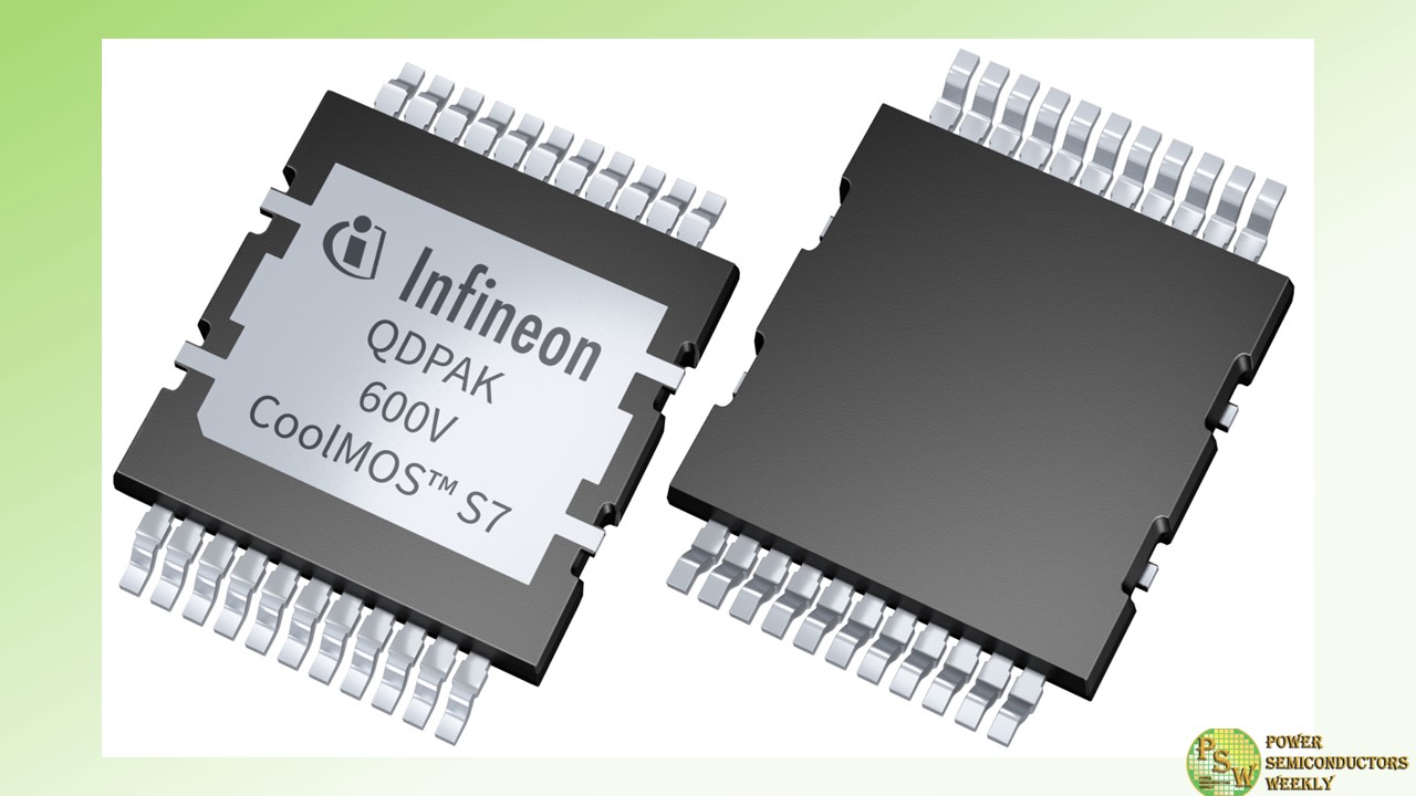
In static switching applications, power designs focus on minimizing conduction losses, optimizing thermal behavior, and achieving compact and lightweight systems while ensuring high quality at a low cost. To meet the needs of next-generation solutions, Infineon Technologies AG is expanding its CoolMOS™ S7 family of high-voltage superjunction (SJ) MOSFETs.
The devices are aiming at SMPS, solar energy systems, battery protection, solid-state relays (SSR), motor-starters and solid-state circuit breakers, as well as PLCs, lighting control, HV eFuse/eDisconnect, (H)EV on-board chargers.
The portfolio extension includes innovative QDPAK top-side cooling (TSC) packages and offers a wide range of features in a small footprint. This makes it highly advantageous for low-frequency switching applications while optimizing cost positioning.
Thanks to the novel high-power QDPAK packaging, they offer an R DS(on) of only 10 mΩ, which is the lowest on the market in this voltage class and the lowest in SMD packages. By minimizing conduction losses of the MOSFETs, the CoolMOS S7/S7A solutions contribute to higher overall efficiency and provide an easy and cost-optimized way to improve system performance.
The CoolMOS S7 power switches also effectively manage heat dissipation with improved thermal resistance. Thanks to the innovative and efficient QDPAK packaging, they also reduce or even eliminate the need for heat sinks in solid-state designs, resulting in more compact and lighter systems.
The MOSFETs are available in both top-side and bottom-side variants, and feature high-pulse current capability, enabling them to handle sudden surges of current. In addition, they exhibit body diode robustness to ensure reliable operation during AC line commutation.
With fewer components required, they reduce part count, resulting in flexible system integration, lower BOM costs, and total cost of ownership (TCO). In addition, these MOSFETs enable shorter reaction times, particularly when breaking a current, facilitating smoother and more efficient operation.
Original – Infineon Technologies
