-
Okmetic CTO Atte Haapalinna gave a speech in September 2023 at the ISES EU Power event on Customized Silicon and SOI Wafers Enabling Enhanced Power Devices.
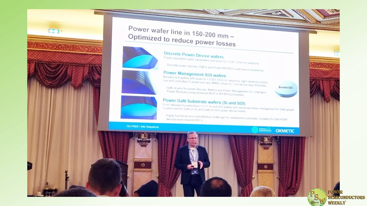
Advanced silicon wafers can greatly improve power device performance and reduce power losses. Okmetic Power wafer line provides an optimal platform for the manufacture of various power devices. Power device optimized wafer solutions improve power device performance, reduce Total Cost of Ownership and enable more refined designs.
Okmetic Power wafer line comprise:
- Power Management SOI wafers (Bonded SOI)
- Power GaN Substrate wafers (Si and SOI)
- Discrete Power Device wafers
Read more about Okmetic’s Power wafer line: Power Wafer Line | Okmetic
Original – Okmetic
-

GaN Systems announced the introduction of its groundbreaking 4th generation GaN power platform. This state-of-the-art technology sets a new power efficiency and compactness standard, delivering an impressive step-function performance boost and industry-leading figures of merit. For example, with GaN Systems Gen4 in an artificial intelligence (AI) server rack, 3.2kW power supplies at 100W/in3 in 2022 are now achieving 120W/in3 with efficiencies above Titanium levels. Gen4 will revolutionize power markets, including consumer electronics, data centers, solar energy, industrial applications, and automotive.
The Gen4 platform also delivers more total bill of material cost savings compared to traditional Silicon and Silicon Carbide solutions, making GaN Systems’ technology a powerful choice for businesses seeking to enhance their competitive advantage.
“Our lead customers have already realized the benefits of our Gen4 platform,” stated Jim Witham, CEO of GaN Systems. “This platform is a testament to our ongoing commitment to continuously delivering superior performance advantages and next-generation levels of efficiency. GaN Systems, in strategic collaboration with industry leaders like TSMC, has invested significantly to meet the ever-evolving demands of our customers. We are pioneering a transformation in product offerings, packaging innovations, enriched functionalities, and unparalleled performance across our markets.”
A Huge Leap for Power Electronics Technology
The Gen4 power platform boasts the following benefits:
- >20% improvement in input and output figures-of-merit translates into reduced losses, enhanced efficiency, and more cost-effective solutions.
- Increased granularity in device specification, combined with a wide range of packaging options, including PDFN, TOLL, TOLT, and Embedded – allowing the correct Rds resistance and package combination for each application, consequently optimizing electrical and thermal system performance.
- 700V E-mode with the industry’s highest transient voltage rating, 850V, significantly enhancing total system reliability and robustness. This rating enables the semiconductor components to withstand user environment anomalies, such as voltage spikes, ensuring uninterrupted and dependable performance.
- On-state resistance ranges enable power systems from 20W to 25,000W.
For more information, visit https://gansystems.com/gan-transistors/gen-4/
Original – GaN Systems
-

Researchers at the Indian Institute of Science (IISc) have developed a fully indigenous gallium nitride (GaN) power switch that can have potential applications in systems like power converters for electric vehicles and laptops, as well as in wireless communications. The entire process of building the switch – from material growth to device fabrication to packaging – was developed in-house at the Centre for Nano Science and Engineering (CeNSE), IISc.
Due to their high performance and efficiency, GaN transistors are poised to replace traditional silicon-based transistors as the building blocks in many electronic devices, such as ultrafast chargers for electric vehicles, phones and laptops, as well as space and military applications such as radar.
“It is a very promising and disruptive technology,” says Digbijoy Nath, Associate Professor at CeNSE and corresponding author of the study published in Microelectronic Engineering. “But the material and devices are heavily import-restricted … We don’t have gallium nitride wafer production capability at commercial scale in India yet.” The know-how of manufacturing these devices is also a heavily-guarded secret with few studies published on the details of the processes involved, he adds.
Power switches are used to control the flow of power to – essentially turn on or off – electronic devices. To design the GaN power switch, the IISc team used a metal organic chemical vapour deposition technique developed and optimised over a decade by researchers in the lab of Srinivasan Raghavan, Professor and Chair, CeNSE. It involves growing GaN alloy crystals layer by layer on a two-inch silicon wafer to fabricate a multi-layered transistor.
The entire process needs to be carried out carefully in a clean room to ensure that no defects arise due to environmental conditions like humidity or temperature, which can affect device performance. The team also took the help of Kaushik Basu, Associate Professor in the Department of Electrical Engineering (EE), and his lab, to build an electrical circuit using these transistors and test their switching performance.
GaN transistors typically operate in what is called a “depletion mode” – they are on all the time unless a negative voltage is applied to turn them off. But power switches used in chargers and adapters need to work the other way around – they normally need to be off and not carrying current, and should only turn on when a positive voltage is applied (“enhancement mode”). To achieve this operation, the team combined the GaN transistor with a commercially available silicon transistor to keep the device normally off.
“The packaging of the device was also indigenously developed,” explains Rijo Baby, PhD student at CeNSE and first author of the study. After packaging and testing, the team found the device performance to be comparable to state-of-the-art switches available commercially, with a switching time of about 50 nanoseconds between on and off operations.
Going forward, the researchers plan on scaling up the device dimensions so that it can operate at high currents. They also plan to design a power converter that can step up or step down voltages.
“If you look at strategic organisations in India, they have a hard time procuring GaN transistors … It is impossible to import them beyond a certain quantity or power/frequency rating,” says Nath. “This is essentially a demonstration of indigenous GaN technology development.”
Original – Indian Institute of Science (IISc)
