-
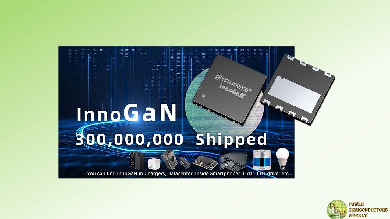
Innoscience Technology has shipped more than 300 million pieces of its InnoGan gallium nitride chips as of August 2023, helping customers achieve small size, high energy efficiency, and low loss product design.
This is in response to phenomenal market demand across multiple sectors multiple applications in the consumer category – fast charging, mobile phones, LEDs – as well as automotive LIDAR, data centres, and renewable energy and energy storage systems, which has seen analysts such as TrendForce’s in its 2023 GaN Power Semiconductor Market Analysis Report, state that “the global GaN power device market will grow from US$180 million in 2022 to US$1.33 billion in 2026, with compound growth rate of 65%”.
In November 2017, Innoscience began the world’s first 8-inch GaN-on-Si mass production line, adopting the Integrated Device Manufacturer (IDM) whole industry chain model, and launched its first low-voltage GaN power device in May 2018. By June 2019, Innoscience’s 650V high-voltage GaN device had passed JEDEC approval, and subsequently, Innoscience has been the only semiconductor company in the world that simultaneously mass-produces high-voltage and low-voltage GaN.
Market acceptance of Innoscience’s high quality, high performance GaN devices has been swift. Following its 2019 entry into the fast charging market, Innoscience’s 650V parts have been adopted in 30W-120W designs by leading brands including ASUS, Anker, Nubia, Baseus, Greenlink, and Flash.
In 2020, Innoscience’s 100V low-voltage GaN was successfully used by Hesai in mass-production LIDAR designs, allowing lasers to achieve image transmission in a shorter time.
In March 2021, the Tencent×Nubia Red Magic mobile phone 6Pro was released. It comes equipped as standard with industry’s first 120W Black Rubik’s Cube GaN fast charge, which is based on Innoscience’s 650V chip. With the successive adoption by Oppo, Vivo, Lenovo and other manufacturers, it has become an industry trend for mobile phones to be equipped with GaN fast charging as standard.
March 2021 saw the mass-production of Innoscience’s bi-directional conduction chip V-GaN officially begin; this device is the only GaN chip in the world that can be applied to high-voltage side load switches, smartphone USB/wireless charging ports with built-in OVP protection, multi-power supply system switch circuits, and other scenarios:one V-GaN replaces two Si MOSFETs in load switching applications resulting in a smaller and more efficient solution.
In October of the same year, Innoscience scored another industry first, as OPPO used the company’s self-developed bi-directional conduction VGaN IC as the internal power switch in its latest smart phone. Other mobile phone makers such as Realme, OnePlus, Lenovo, and Motorola have also successively adopted VGaN for charging protection.
In May 2022, Shounuo released the world’s smallest 45W/65W PD car charger, using Innoscience’s 40V low-voltage INN040FQ043A.
Then in July, Anker and Innoscience jointly released the world’s first 65W full-GaN fast charger. This design uses GaN power chips at both the AC and DC ends for the first time, taking system power density and efficiency to a whole new level.
Later, in October 2022, Innoscience achieved mass production of GaN products targeting industrial power supplies – again an industry first – comprehensively improving energy conversion efficiency and reducing system energy consumption.
In November 2022, Innoscience’s INN100W032A won the IIC World Electronics Achievement Award. The gate charge of this product is only 20% of a traditional silicon MOSFET, and its Ciss is only 40% of its silicon counterpart. It can be widely applied in motor drive, Class D, data centre, motor-driver, communication base station and other product fields. In January 2023, Innoscience launched the SolidGaN ISG3201, a 100V highly-integrated half-bridge drive packaged solution, further improving the overall system performance of 48V power supply of data centre module power supplies, motor drives, class D power amplifiers, photovoltaic inverters and light hybrid electric vehicles.
The move to GaN as the premium power semiconductor technology is driven both by new GaN products and market demands. As an example, in April this year, Innoscience’s IATF 16949 automotive-grade low-voltage parts successfully expanded from industrial to automotive applications, with use in autonomous vehicle LIDAR systems.
Then in July 2023, Innoscience began to apply GaN in the field of renewable energy, reducing the size and improving the efficiency of photovoltaic modules.
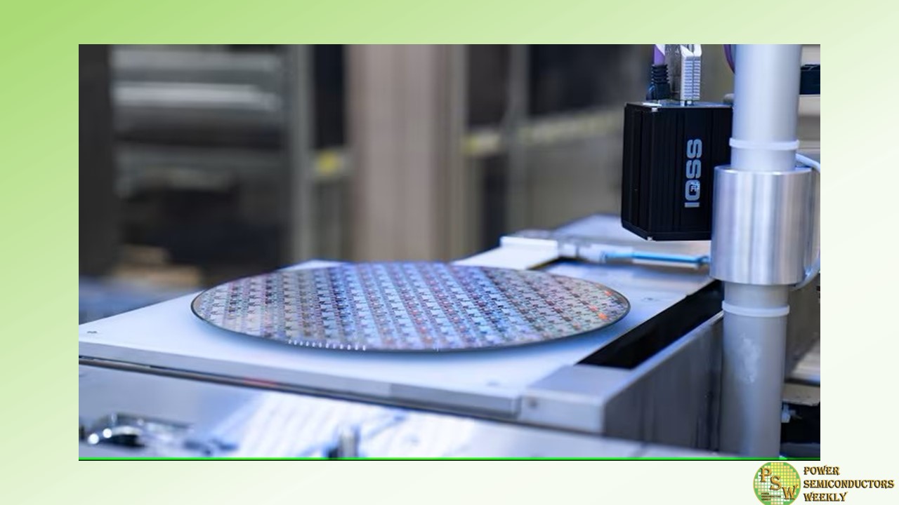
By the end of August 2023, Innoscience had successfully mass-produced 54 different types of high-voltage GaN chips (650V-700V) and 20 types of medium-low voltage GaN chips (30V-150V). Products span three chip categories: wafers, discrete devices and integrated solutions.
Commented Dr Denis Marcon, Innoscience’s General Manager, Europe: “We are just at the start of the GaN story. The first applications were all in consumer, but GaN is undoubtedly the key to reducing costs and increasing efficiency in the industrial field as well. And according to automotive industry forecasts, GaN may enter automotive market already this year penetrating applications such as low-power OBC and DC-DC applications in 2025.
With such rapid growth in market demand, the reliability of devices, price competitiveness and stable supply in large quantities are now the major concerns of users. Based on an advanced Innoscience’s 8-inch GaN-on-Si IDM manufacturing platform, Innoscience’s current production capacity has reached 15,000 wafers per month, providing tremendous advantages in scale, reliability and cost.”
Original – Innoscience Technology
-
NXP Semiconductors N.V. announced it is strengthening its European research and development (R&D) through grants to be provided via the 2nd Important Project of Common European Interest on Microelectronics and Communication Technologies (IPCEI ME/CT), with the final investment decision pending confirmation of the level of public funding. Dedicated NXP teams across Austria, Germany, the Netherlands and Romania will innovate in core technologies across automotive, industrial and cybersecurity. This includes 5nm, advanced driving assistance and battery management systems in automotive, 6G and Ultra-Wideband as well as artificial intelligence (AI), RISC-V and post-quantum cryptography.
“NXP’s planned investments in our Austrian, German, Dutch, and Romanian operations signal our strong commitment to the EU’s goal of enabling both digital and green transition. Our activities through IPCEI ME/CT complement NXP’s planned joint venture participation in TSMC’s first European foundry. It also underscores our commitment to strengthening innovation and supply chain resilience in Europe. NXP believes expanding research, development, and manufacturing efforts in Europe is of vital importance, and each of these three critical elements must be successfully integrated to achieve greater European semiconductor ecosystem resilience.”
Kurt Sievers, President and CEO of NXP
Extensive research, development, and manufacturing presence across multiple sites in all four countries enable NXP to develop cutting-edge technology and products that contribute significantly to the achievement of EU industrial strategies. In close collaboration with a strong ecosystem of more than 50 partners from industry and academia across Europe, NXP will strengthen key technologies of microelectronics in Europe.
No other microelectronics company participating in IPCEI ME/CT is currently planning to invest in its operations across so many EU member states. NXP is also an active participant in three of the four IPCEI ME/CT workstreams: “Sense”, “Think”, and “Communicate”, reflecting NXP’s areas of leadership and strategic focus.
NXP’s planned investments in Austria, Germany, the Netherlands, and Romania follow the announcement that the company is going to form a new joint venture, ESMC (European Semiconductor Manufacturing Company), with TSMC, Bosch, and Infineon with plans to establish TSMC’s first semiconductor manufacturing site in Europe. The new 300mm fab, planned to be built in Dresden, Germany, is expected to have a monthly production capacity of 40,000 300mm (12-inch) wafers on TSMC’s 28/22 nanometer planar CMOS and 16/12 nanometer FinFET process technology, further strengthening Europe’s semiconductor manufacturing ecosystem with advanced FinFET transistor technology and creating about 2,000 direct high-tech professional jobs.
NXP in Austria
NXP Austria is a center of excellence for cryptography and security, advancing solutions that make lives easier, better and safer. NXP Austria innovates hardware and software solutions as well as services for the IoT, automotive, Industry 4.0 and mobile sectors. At NXP Austria, nearly 800 people from approximately 50 countries work on Innovations to research, design, develop, manage, and promote NXP’s products.
For more information on NXP in Austria, visit nxp.com/austria
NXP in Germany
With over 1,200 people, Germany is a very important R&D hub for NXP with a focus on semiconductor solutions for the automotive market as well as secure connected edge applications, such as industrial IoT, mobile, and wearables. Primary R&D competencies in Hamburg, Munich, and Dresden include cybersecurity, automotive processing, and RF. A collaborative quantum computing initiative was established in 2023 in Hamburg. IPCEI will help to further strengthen and expand these core competencies. In addition, the German sites are home to an experienced sales engineering team that completes NXP’s global network of customer support.
For more information on NXP in Germany, visit nxp.com/germany
NXP in the Netherlands
NXP has over 2,200 people and significant operations across three sites in the Netherlands. NXP’s international headquarters is located on the High Tech Campus Eindhoven. R&D groups based in Eindhoven focus on security innovation, software and hardware IP development, chip design, system innovation and certification. NXP Nijmegen features manufacturing, R&D, testing, technology enablement and support functions. NXP’s Delft site is home to hardware and software design teams focusing on secure wireless solutions including automotive electronics such as radio, GPS, car access systems, and sensor electronics.
For more information on NXP in the Netherlands, visit nxp.com/netherlands
NXP in Romania
NXP Bucharest’s over 1,000 people focus on software development for automotive, microcontrollers and connectivity products as well as IT service management and customer supply operations. Each year, NXP Romania hosts interns who learn the specifics of software development in automotive, edge computing and IoT.
For more information on NXP in Romania, visit nxp.com/romania
Original – NXP Semiconductors
-
Nicolas Dufourcq, Chairman of the Supervisory Board of STMicroelectronics N.V., and Maurizio Tamagnini, Vice-Chairman, have asked Jean-Marc Chery, ST’s President and CEO, to be available for a reappointment in his current role. Mr. Chery has accepted the proposal.
Therefore, the Supervisory Board has decided to propose for shareholder approval at the Company’s 2024 Annual General Meeting of Shareholders, the reappointment for a three-year mandate of Jean-Marc Chery as the sole member of the Managing Board and the Company’s President and Chief Executive Officer.
The decision recognizes the importance of the continuity of ST’s strategy, execution and value proposition under Mr. Chery’s leadership.
Original – STMicroelectronics
-
IQE plc, the leading supplier of compound semiconductor wafer products and advanced material solutions to the global semiconductor industry, announced a strategic collaboration with VisIC Technologies, a global leader in the provision of GaN (Gallium Nitride) power solutions to the automotive sector, to develop the highest reliability gallium nitride D-Mode (D-Mode GaN) power products for use in electric vehicles inverters.
IQE and VisIC Technologies will collaborate to develop 200mm (8”) D-Mode GaN power epiwafers that will be developed at IQE’s UK facilities, leveraging IQE’s well-established expertise in GaN technology.
VisIC Technologies, with its ground-breaking D3GaN technology (Direct Drive D-Mode GaN), brings the future of EV inverters into focus. This technology promises to reduce power consumption, increase reliability and enhance performance in electric vehicles. By combining VisIC Technologies’ innovative Power Electronics solutions with IQE’s epitaxy excellence, this partnership aims to accelerate the adoption of GaN-on-Silicon technology in EVs, significantly contributing to the evolution of sustainable transportation.
The collaboration marks another important milestone in IQE’s strategy of diversification into the high-growth Power market, first announced at its 2022 Capital Markets Day. IQE sees significant opportunities in the GaN Power epiwafer market in particular, which is forecast to reach a $632m value by 2027.
Original – VisIC Technologies
