-

Aehr Test Systems announced it has received an initial customer order for a FOX-NP™ wafer level test and burn-in system, multiple WaferPak™ Contactors, and a FOX WaferPak Aligner to be used for engineering, qualification, and small lot production wafer level test and burn-in of their silicon carbide devices. The customer is a US-based multibillion-dollar semiconductor supplier serving several markets including automotive, computing, consumer, energy, industrial, and medical. The FOX-NP system, including the FOX WaferPak Aligner and initial WaferPaks are scheduled per the customer’s requested accelerated schedule to ship by the end of the calendar year 2023.
The FOX-NP system is configured with the new Bipolar Voltage Channel Module (BVCM) and Very High Voltage Channel Module (VHVCM) options that enable new advanced test and burn-in capabilities for silicon carbide power semiconductors using Aehr’s proprietary WaferPak full wafer Contactors. This new order highlights Aehr’s continued progression within the growing silicon carbide global power market.
Gayn Erickson, President and CEO of Aehr Test Systems, commented, “We are very excited that after conducting a detailed financial evaluation and multiple onsite visits to Aehr’s application lab, this new customer selected our FOX-P solution for engineering, qualification, and production of their silicon carbide power devices.
This evaluation included cost of ownership and system throughput, as well as device test, burn-in, and stabilization coverage. As their production capacity increases, they told us that they will quickly move to our FOX-XP multi-wafer test and burn-in systems for high-volume production. In addition to the automotive electric vehicle device opportunity, this customer in particular sees the enormous opportunity for silicon carbide power devices in industrial, solar, and other power applications.
“William Blair forecasts that in addition to the 4.5 million six-inch equivalent wafers that will be needed to meet the demand for electric vehicle related silicon carbide devices in 2030, another 2.8 million wafers are needed to address industrial, solar, electric trains, energy conversion and other applications in 2030. The interesting part of this is that most of these applications will be served with discrete MOSFETS in single die packages.
The cost of ownership of our solution proved to be more cost-effective and efficient for these devices than package part burn-in after the die are packaged in packages such as TO-247 or other discrete packages. This is a strong testimony of the advantage of wafer level burn-in as a better alternative to package part burn-in. This expands our silicon carbide test and burn-in market even more and this new customer helps expand Aehr’s presence in this market as our total addressable market (TAM) continues to grow.
“Aehr’s FOX-P systems and proprietary WaferPak full wafer Contactors enable our customers to do economical production volume test and reliability burn-in with processes such as High Temperature Gate Bias (HTGB) and High Temperature Reverse Bias (HTRB) very cost-effectively and ensure extremely high device quality. Our systems are typically used for long burn-in times lasting up to 24 hours or more.
We can do this for under $5.00 per hour per wafer capital depreciation cost while testing and burning-in up to several thousand devices at a time per wafer. This is also in a test system footprint that is up to 94% less than a typical test system on a standard semiconductor wafer prober, which in a precious clean room wafer facility is extremely important and saves a great deal of cost.
“The FOX family of compatible systems including the FOX-NP and FOX-XP multi-wafer test and burn-in systems and Aehr’s proprietary WaferPak full wafer contactors provide a uniquely cost-effective solution for burning in multiple wafers of devices at a single time to remove early life failures of silicon carbide devices, which is critical to meeting the initial quality and long-term reliability of the automotive, industrial, and electrification infrastructure industry needs.”
The FOX-XP and FOX-NP systems, available with multiple WaferPak Contactors (full wafer test) or multiple DiePakTM Carriers (singulated die/module test) configurations, are capable of functional test and burn-in/cycling of devices such as silicon carbide and gallium nitride power semiconductors, silicon photonics as well as other optical devices, 2D and 3D sensors, flash memories, magnetic sensors, microcontrollers, and other leading-edge ICs in either wafer form factor, before they are assembled into single or multi-die stacked packages, or in singulated die or module form factor.
Original – Aehr Test Systems
-
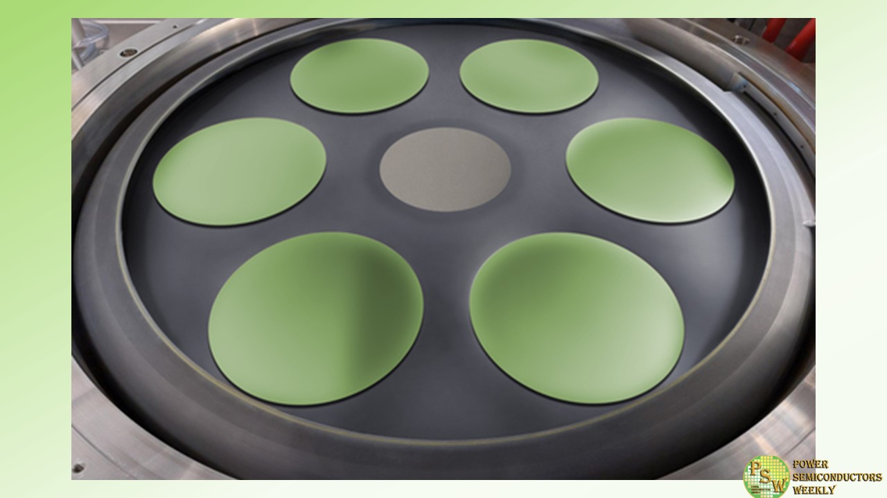
AIXTRON SE supports GlobiTech Inc., one of the world’s largest silicon-epitaxy foundries, to expand their business into silicon carbide (SiC) epitaxy. AIXTRON’s new G10-SiC has enabled this global leader to quickly ramp its SiC epitaxy production into high volume to address the world’s increasing demand for power epi-wafers. GlobiTech’s selection of the G10-SiC means a future-proof investment based on dual wafer size configuration of 9×150 & 6×200 mm and the highest throughput per fab space available in the SiC industry today.
The G10-SiC was officially introduced in September 2022. And it has quickly become the tool of record for both 150mm and 200mm SiC device makers as well as foundries like GlobiTech, the wholly owned subsidiary of GlobalWafers Co., Ltd., which manufactures silicon carbide and silicon epitaxial wafers focused on power and electric vehicle (EV) market segments.
“When one of the largest manufacturers and foundries like GlobiTech diversifies its business, it is a clear signal of a long-lasting trend in the semiconductor industry: conventional silicon is being replaced by silicon carbide in an ever-increasing number of applications. And it makes us proud when a leading company such as GlobiTech chooses AIXTRON and our new G10-SiC as an enabler of its transition intothis emerging SiC market. It confirms our overall strategy and the prospects for further growth”, says Dr. Felix Grawert, CEO and President of AIXTRON SE.
GlobiTech, located in Sherman, TX, is already in high-volume production using both G5WW C and G10-SiC AIXTRON systems, with continued installation capacity over the next years.Modeled after the silicon business, GlobiTech supplies both SiC substrates and SiC epitaxy to the market.
“In AIXTRON, we have found a strong partner supporting us in our vision and plans to expand our business into the SiC epitaxy market – an important step as SiC technology is one of the fastest-growing semiconductor sectors. AIXTRON tools allow us to get the most wafers out of our current fab. And AIXTRON’s team understands what it takes to compete against silicon to grow this market while offering great customer support and service”, says Mark England, President of GlobalWafers.
The G10-SiC is the first SiC epitaxy tool on the market that truly enables high-volume production of SiC epi-wafers. Since the G10-SiC offers both 9×150 mm and 6×200 mm batch configurations, it is an instrumental tool for a market rapidly transitioning from 6-inch (150mm) to 8-inch (200 mm) wafer diameters. The new platform is built around AIXTRON’s proven automated wafer cassette-to-cassette loading solution with high-temperature wafer transfer.
Combined with high growth rate process capabilities, the G10-SiC provides best-in-class wafer throughput, an excellent epi wafer performance in terms of quality and uniformity, and the best throughput per square meter of fab space. All this leads to the lowest cost of ownership in the market. It is estimated that in 2023, the new G10-SiC will become AIXTRON’s top-selling product.
The wide-bandgap material SiC is set to become mainstream technology for efficient power electronics. Driven by the growing adoption of SiC-based power semiconductors within e-mobility solutions and the overall acceleration of the charging infrastructure, the global demand for SiC wafers is growing rapidly.And with its superior characteristics, SiC semiconductors offer higher energy efficiency than conventional power electronics based on silicon. Therefore, SiC significantly contributes to reducing the global CO2 footprint.
Original – AIXTRON
-
Semilab announced an agreement to form a long-term strategic partnership with Fraunhofer IISB. Within the framework of this cooperation, a demo lab will be opened with a strong focus on developing state-of-the-art metrology and inspection solutions for wide bandgap semiconductor materials.
Over the years, developments in compound semiconductor materials such as silicon carbide (SiC) have been receiving increased attention. SiC devices show great promise in the future of wide bandgap semiconductors due to their superior material properties. The silicon carbide market’s growth shows no sign of slowing down due to the expansion in the industrial and automotive sectors. Semilab believes in driving decarbonization by supporting the development of key SiC products and components.
Based in Budapest, Hungary, Semilab is a strategic metrology supplier and innovation partner of the leading wafer manufacturers, IC device makers in the More-than-Moore market segment. Semilab provides state-of-the-art metrology solutions for semiconductor device manufacturers, both in-line and R&D segments. The company is among the world leaders in non-contact CV metrology for SiC and its market share is growing for EPI thickness and resistivity monitoring.
The Fraunhofer IISB in Erlangen, Germany, specializes in wide-bandgap semiconductors and efficient power electronics. Here, device know-how merges with complex system development, especially for e-mobility and sustainable energy supply.
The institute bundles its activities in the two business units Power Electronic Systems and Semiconductors. In doing so, it comprehensively covers the entire value chain from basic materials, through semiconductor device, process and module technologies, to complete electronics and energy systems. As a unique center of excellence in Europe for the semiconductor material silicon carbide (SiC), the IISB is a pioneer in the development of highly efficient power electronics, even for extreme requirements. This spans from material, over process and to device development supported by providing innovative metrology solutions.
Considering the crucial role both players have in shaping of the European semiconductor scene, the strategic partnership between Semilab and Fraunhofer IISB will allow the utilization of their respective resources and global networks in order to develop new, innovative silicon carbide processes and metrologies.
Original – Semilab
