-
Mitsubishi Electric Corporation announced that it has developed a new structure for a silicon carbide metal-oxide-semiconductor field-effect transistor (SiC-MOSFET) embedded with a Schottky barrier diode (SBD), which the company has applied in a 3.3 kV full SiC power module, the FMF 800 DC -66 BEW for large industrial equipment such as railways and DC power systems. Samples began shipping on May 31. The chip’s new structure is expected to help downsize railway traction systems, etc. as well as make them more energy efficient, and contribute to carbon neutrality through the increased adoption of DC power transmission.
SiC power semiconductors are attracting attention with their capacity to significantly reduce power loss. Mitsubishi Electric, which commercialized SiC power modules equipped with SiC-MOSFETs and SiC-SBDs in 2010, has adopted SiC power semiconductors for a variety of inverter systems, including air conditioners and railways.
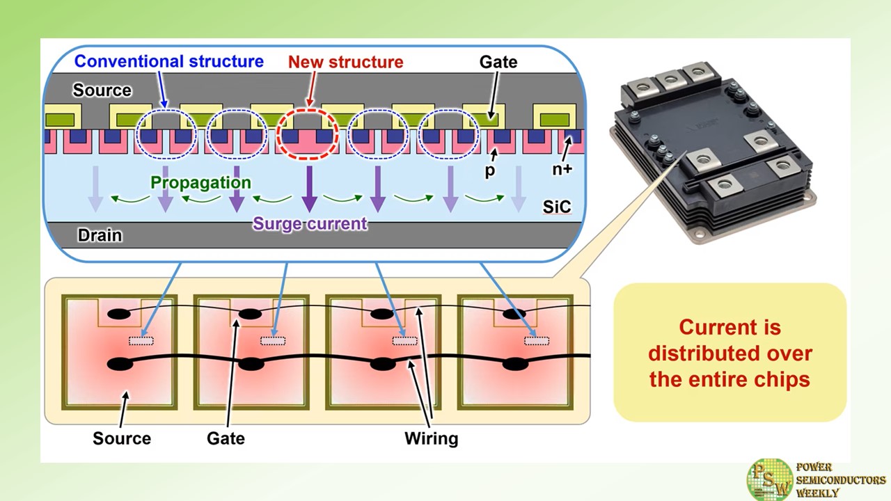
The chip integrated with a SiC-MOSFET and a SiC-SBD can be mounted on a module more compactly compared to the conventional method of using separate chips, thus enabling smaller modules, larger capacity, and lower switching loss. It is expected to be widely used in large industrial equipment such as railways and electric power systems. Until now, the practical application of power modules with SBD-embedded SiC-MOSFETs has been difficult due to their relatively low surge-current capability, which results in the thermal destruction of the chips during surge-current events because surge currents in connected circuits concentrate only in specific chips.
Mitsubishi Electric has now developed the world’s first mechanism by which surge current concentrates on a specific chip in a parallel-connected chip structure inside a power module, and a new chip structure in which all chips start energizing simultaneously so that surge current is distributed throughout each chip. As a result, the power module’s surge-current capacity has been improved by a factor of five or more compared to the company’s existing technology, which is equal to or greater than that of conventional Si power modules, thus enabling the application of an SBD-embedded SiC-MOSFET in a power module.
Original – Mitsubishi Electric
-

A team of scientists from GE Research have set a new record, demonstrating SiC MOSFETs (Metal–Oxide–Semiconductor Field-Effect Transistors) that can tolerate temperatures exceeding 800 degrees C. This at least 200 degrees C higher than previously known demonstrations of this technology and shows the potential of SiC MOSFETs to support future applications in extreme operating environments. It also defies what most electronics experts believed was achievable with these devices.
As GE’s Aerospace business looks to continuously improve the state-of-the-art in aviation systems for its existing commercial and military customers and seeks to enable new applications in support of space exploration and hypersonic vehicles, building a portfolio of electronics that can function in extreme operating environments will be essential. For more than three decades, GE has built a world leading portfolio in SiC technology and sells an array of SiC-based electrical power products through the Aerospace business for aerospace, industrial and military applications.
Emad Andarawis, a Principal Engineer in Microelectronics at GE Research, says achieving the high temperature threshold with SiC MOSFETs could open a whole new aperture of sensing, actuation and control applications for space exploration and hypersonic vehicles, stating, “We know that to break new barriers with space exploration and hypersonic travel, we will need robust, reliable electronics systems that can handle the extreme heat and operating environments. We believe that we have set a record, demonstrating 800 degree C SiC MOSFETS that represents a key milestone toward these mission critical goals.”
GE’s SiC MOSFETs could support the development of more robust sensing, actuation and controls that open new possibilities in space exploration and enable the control and monitoring of hypersonic vehicles traveling at speeds of MACH 5, or greater than 3,500 MPH. That is more than six times the speed that a typical commercial passenger flight travels today.
Andarawis noted that the electronics industry has seen a number of exciting developments in high temperature electronics with SiC. The National Aeronautics and Space Administration (NASA) has demonstrated SiC JFETs that have tolerated well beyond the 800 degree C threshold. For a long time, the conventional wisdom has been that SiC MOSFETs cannot offer the same degrees of reliability and durability as JFETs at high temperatures. New advancements with the gate oxides in SiC MOSFETS, which have previously been temperature and lifetime limiters, have narrowed the gap considerably.
The recent demonstration of Andarawis and the GE Research shows that MOSFETs could expand the portfolio of available options to consider. This builds on a growing body of work in SiC-enabled electronics that GE Aerospace researchers are at the forefront of leading. The team is currently collaborating on a project with NASA to apply novel SiC photodiode technology to develop and demonstrate a Ultraviolet imager that enhances space missions to the surface of Venus. GE research teams also are fabricating NASA’s JFETs in our cleanroom facility as part of work they are doing for an external semiconductor partner.
The cleanroom facility is a major focal point of GE’s research in SiC. It is a 28,000 sq. ft., Class 100 (ISO 9001 certified) facility, based on GE’s research campus in Niskayuna, NY. The facility can support technology from R&D through low-volume production and transfer technology to high-volume manufacturing supporting GE internal products or select external commercial partners (www.ge.com/research/). Andawaris said, “GE’s Cleanroom facility is a tremendous research, prototyping and production asset that is allowing us to rapidly develop and scale promising electronics platforms like SiC MOSFETs. We are excited about the road ahead as we support GE Aerospace’s efforts to redefine air travel in the skies and beyond.”
Original – GE Research
