-
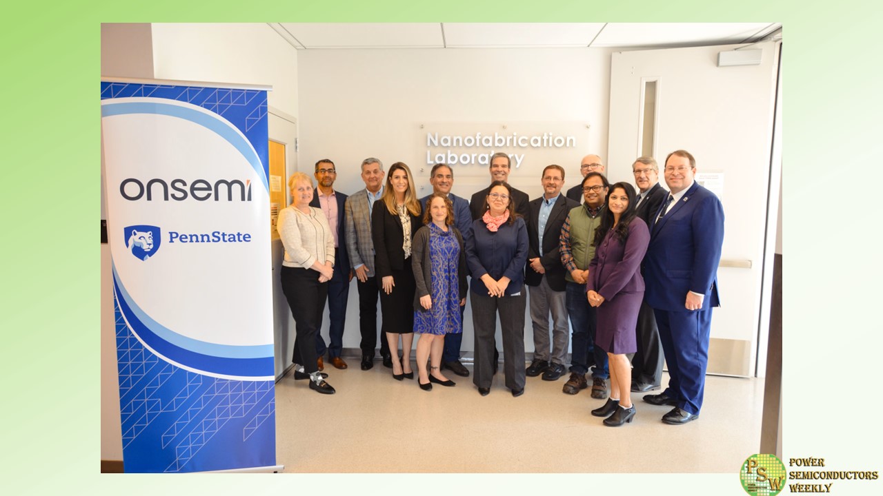
Penn State and onsemi, a leader in intelligent power and sensing technologies, announced the signing of a memorandum of understanding (MOU) towards an $8 million strategic collaboration which includes the establishment of the onsemi Silicon Carbide Crystal Center (SiC3) at Penn State’s Materials Research Institute (MRI). onsemi will fund SiC3 with $800k per year over the next 10 years.
Silicon carbide (SiC) is vital for enabling efficiency in electric vehicles (EVs), EV charging and energy infrastructure and contributes to the decarbonization of the global economy. Academic research in SiC made great advancements in the late 1990s and early 2000s, but has since diminished in the U.S. This agreement will put SiC crystal research in America back on the map.
In addition to conducting SiC research at SiC3, Penn State and onsemi will raise awareness about the increasing demand for tech jobs in the semiconductor industry. This is part of their efforts to enhance the share of U.S. semiconductor manufacturing. They also will partner on workforce development initiatives such as internship and cooperative programs and include SiC and wide bandgap crystal studies in Penn State’s curriculum. The relationship with Penn State is part of onsemi’s commitment to promoting STEAM (Science, Technology, Engineering, Arts, and Mathematics) education, ranging from helping K-12 students in underserved communities to university collaborations that support the development of the workforce for today and the future.
Lora Weiss, Penn State senior vice president of research, noted that the Penn State-onsemi collaboration is a match that makes perfect sense given each entity’s demonstrated strengths.
“onsemi is a proven innovator, delivering a comprehensive portfolio of intelligent power and sensing technologies to enable and accelerate sustainable solutions across multiple markets,” Weiss said. “At the same time, as per the National Science Foundation’s research expenditure rankings, Penn State is ranked first in materials science and second in materials engineering. We have world-class nanofab and characterization facilities that support research on thin films, silicon carbide and other materials used in semiconductors and other technologies. These complementary capabilities between onsemi and Penn State will have a strong impact on research and development, economic growth, and workforce development.”
Penn State’s capabilities make them an ideal academic partner for onsemi to advance the state of the art in silicon crystal growth.
“Penn State is uniquely positioned to rapidly establish a silicon carbide crystal growth research program,” said Pavel Freundlich, chief technology officer, Power Solutions Group, onsemi. “The university offers a wide breadth of capability based on its current materials research, wafer processing capabilities in its nanofab facility, and a comprehensive, world-class suite of metrology instrumentation.”
The relationship developed over a period of due diligence during which it became clear that their cooperative efforts would position Penn State and onsemi as leaders in SiC research.
“Over the next decade, this collaboration will enable Penn State to become the nation’s leading resource for semiconductor crystal science and workforce development,” said Justin Schwartz, Penn State executive vice president and provost. “And this would not be possible without the relationship-building efforts of Priya Baboo, senior director of corporate and industry engagement, and the technical expertise of Joshua Robinson, professor of materials science and engineering, and their counterparts at onsemi.” Scott Allen, vice president, University Relations, onsemi, added that “Penn State’s expansion of its curriculum to offer specialty courses in SiC and wideband gap technology will play a key role in meeting onsemi’s strategic workforce development goals and help to meet American semiconductor workforce goals as outlined in the recently signed CHIPS and Science Act.”
Original – onsemi
-
AIXTRON SE plans to invest up to 100 million euros at its Herzogenrath site. A new innovation center is to be built, which will provide the manufacturer of deposition equipment to the semiconductor industry with enhanced capacities for research and development. AIXTRON received approval for the new project from the company’s Supervisory Board.
The new innovation center will provide 1000m2 of cleanroom space and will be built on the company’s premises in Herzogenrath, Germany. The new building will create further capacities for the next product generations which are already in preparation, as well as for further product developments beyond that.
“With our products, we address the megatrends of digitalization, electromobility and energy efficiency and are experiencing a strong and steadily growing demand. Technical innovations and product developments that precisely address the needs of our customers are the key to our success. And our dynamic environment offers us further growth opportunities,” says Dr. Felix Grawert, CEO of AIXTRON SE. “We are therefore very pleased that the Supervisory Board has approved this project which will enable us to create the foundation for further product developments and for future growth.”
The importance of product development in the dynamic semiconductor industry is demonstrated by the success of AIXTRON’s new “G10” system generations. In the first year after market introduction, AIXTRON expects to generate more than 40 percent of its annual revenues with this new product generation. Right after its official launch, the new tool for the silicon carbide material system (G10-SiC) has already generated a high order intake. And it is expected to continue to drive further growth all throughout 2023 and beyond.
Also, the new AIXTRON solution for the gallium-arsenide/indium-phosphite material system (G10-AsP) which was launched at the beginning of 2023 already enjoys a strong demand. For the first time, it enables the high-volume production of Micro LEDs and photonic components such as lasers on wafers with a diameter of up to 200mm. Later in the year, the new G10 system for gallium nitride (GaN) will also be launched. The material systems SiC and GaN have the potential to fully cover the complete range of power electronics, from electromobility to renewable energy technologies to fast data transmission. With their outstanding material properties, they will ensure a significant reduction in global CO2 emissions in these areas and help electromobility achieve a breakthrough.
Original – AIXTRON
