Okmetic Tag Archive

  • Okmetic Expands Wafer Portfolio with 300mm and Epitaxial Offerings via Partner Network

    Okmetic Expands Wafer Portfolio with 300mm and Epitaxial Offerings via Partner Network

    2 Min Read

    Okmetic has expanded its wafer portfolio to include 300 mm polished wafers and 150–300 mm epitaxial (EPI) wafers through qualified manufacturing partners, strengthening its position as a Europe-based supplier across multiple semiconductor segments.

    The company will continue its in-house production of advanced 150–200 mm silicon and bonded SOI wafers, while leveraging external partners for larger wafer sizes and EPI solutions. Despite outsourcing production, Okmetic retains full responsibility for supply chain management and wafer quality, ensuring consistent performance and customer experience.

    This hybrid manufacturing model enhances supply flexibility and enables Okmetic to address a broader range of applications, including memory, logic, power, RF, and mixed-signal devices. At the same time, the company maintains strong support for its core markets such as MEMS, sensors, and power semiconductors. Notably, Okmetic also continues to support long-term demand for 150 mm wafers, while its expanded 200 mm polished wafer capacity entered volume production in early 2026.

    From a market perspective, this move reflects increasing demand for diversified wafer sourcing strategies, particularly as customers balance legacy nodes (150/200 mm) with advanced 300 mm manufacturing. By combining internal capabilities with partner manufacturing, Okmetic is aligning with industry trends toward supply chain resilience, multi-sourcing, and scalable capacity.

    The expansion also positions Okmetic to better support evolving device architectures, including GaN-on-Si and advanced power devices, where substrate quality and availability remain critical. Ongoing R&D collaboration with customers and research partners further supports future technology roadmaps and next-generation semiconductor applications.

    Original – Okmetic

    Comments Off on Okmetic Expands Wafer Portfolio with 300mm and Epitaxial Offerings via Partner Network
  • Okmetic Joins WIBASE Initiative to Advance Wide Bandgap Power Electronics

    Okmetic Joins WIBASE Initiative to Advance Wide Bandgap Power Electronics

    2 Min Read

    Okmetic is participating in WIBASE (Wide Bandgap Semiconductor Power Electronics), a Finnish initiative focused on accelerating wide bandgap semiconductor technologies for next-generation power electronics. The three-year program aims to strengthen national capabilities spanning device processing, prototyping, integration, packaging, testing and lifetime modelling, supporting the shift toward more efficient and sustainable power conversion.

    Coordinated by VTT Technical Research Centre, the WIBASE consortium brings together ten partners, including six companies and four Finnish research organizations. The industrial participants cover the value chain from advanced materials and thin-film expertise to engineered silicon substrates and end applications in power electronics. The project is funded by Business Finland.

    WIBASE targets several barriers that can slow wide bandgap adoption, including device and module reliability, material defects, thermal management challenges and high-temperature interconnect technologies. The initiative also emphasizes collaboration with leading international research groups and is designed to support technology development, know-how growth and IP creation in wide bandgap power technologies.

    Within WIBASE, Okmetic is working with project partners to develop and characterize optimized silicon substrates for GaN power devices. The company highlighted the role of GaN-on-Si in combining gallium nitride’s high electron mobility, thermal stability and high-voltage capability with silicon’s scalability, stable supply base and cost-efficient high-volume manufacturing potential. Okmetic said its contribution builds on its experience supplying Power GaN Substrate wafers, with the goal of providing a reliable and well-controlled silicon platform aligned with performance and manufacturability requirements.

    Okmetic expects WIBASE to help establish a Finnish expertise cluster in wide bandgap power electronics, reinforcing technological self-sufficiency, strengthening IP creation and improving competitiveness across the semiconductor and power electronics ecosystem. The outcomes are also positioned to benefit the broader power device sector through advances in materials, silicon substrates and manufacturing know-how.

    WIBASE partners in Finland include Okmetic, VTT, Aalto University, LUT University, University of Helsinki, ABB, Picosun, Danfoss Drives, Comptek Solutions and Kempower.

    Original – Okmetic

    Comments Off on Okmetic Joins WIBASE Initiative to Advance Wide Bandgap Power Electronics
  • Okmetic Starts Volume Production at Expanded Vantaa Silicon Wafer Fab in Finland

    Okmetic Starts Volume Production at Expanded Vantaa Silicon Wafer Fab in Finland

    2 Min Read

    Okmetic has entered volume production at its expanded Vantaa fab in Finland. The site focuses on 150–200 mm silicon and bonded silicon-on-insulator (SOI) wafers, with the expansion significantly increasing 200 mm polished wafer capacity.

    “With this expansion, Okmetic strengthens its position as an EU-based, one-stop supplier for 150 to 200 mm silicon wafer platforms serving the MEMS, sensor, RF, and Power markets. The increase in 200 mm polished wafer capacity strengthens long-term supply stability for critical semiconductor applications,” said President and CEO Kai Seikku.

    Okmetic produced the first wafers from the expanded fab in June 2025, launching a structured qualification and ramp phase. With volume production now underway in early 2026, the company has started delivering wafers from the expanded capacity to customers, supporting long-term supply readiness across MEMS, RF, Power and GaN-based applications.

    The Vantaa expansion is part of Okmetic’s broader plan to more than double capacity by 2030. Construction began in early 2023 and adds more than 40,000 m², including a 6,000 m² cleanroom as well as new crystal growth and wafering areas. Okmetic said the fab upgrade incorporates state-of-the-art equipment with a focus on energy efficiency.

    The latest investment builds on prior capacity additions, including the doubling of bonded SOI production capacity between 2017 and 2021 and the introduction of a patterning line for Cavity SOI (C-SOI®) production in 2019. By expanding 200 mm polished wafer output, Okmetic aims to better meet evolving industry demand while reinforcing Europe-based supply of 150–200 mm wafer platforms.

    Original – Okmetic

    Comments Off on Okmetic Starts Volume Production at Expanded Vantaa Silicon Wafer Fab in Finland
  • Okmetic Produces First Wafers from €400M Vantaa Fab Expansion, Doubling 200mm Capacity for MEMS, RF, and Power Devices

    Okmetic Produces First Wafers from €400M Vantaa Fab Expansion, Doubling 200mm Capacity for MEMS, RF, and Power Devices

    2 Min Read

    Okmetic has successfully produced the first wafers from its new Vantaa fab expansion in Finland. Okmetic Vantaa fab focuses on 150-200 mm silicon and bonded silicon-on-insulator (SOI) wafers with large fab expansion adding 200 mm polished wafer capacity significantly.

    The completion of the first phase of what will ultimately be 400 million euro expansion, the largest investment in company history, is a significant milestone coinciding with Okmetic’s 40th anniversary. With the first wafers successfully produced, the company is now preparing for sample deliveries to customers, marking the next step in ramping up production.  

    Vantaa site Fab expansion is set to more than double Okmetic capacity by 2030. The construction of the expansion began in early 2023. Spanning over 40,000 m², the expansion includes a 6,000 m² cleanroom area along with crystal growth and wafering areas. The fab expansion is equipped with state-of-the-art technology, with focus on energy efficiency.   

    Building on previous investments, Okmetic has significantly expanded its manufacturing capabilities in recent years, including doubling bonded SOI production capacity between 2017 and 2021 and adding a patterning line for Cavity SOI (C-SOI®) production in 2019. 

    This latest expansion further strengthens Okmetic’s ability to meet growing semiconductor industry demands. By significantly increasing 200 mm polished wafer capacity, it reinforces Okmetic’s position as a leading supplier of advanced silicon wafers based in Europe, ensuring a stable and high-quality supply of 150–200 mm wafers.

    Original – Okmetic

    Comments Off on Okmetic Produces First Wafers from €400M Vantaa Fab Expansion, Doubling 200mm Capacity for MEMS, RF, and Power Devices
  • Okmetic Celebrates 25th Anniversary of its North American Sales Office in Texas

    Okmetic Celebrates 25th Anniversary of its North American Sales Office in Texas

    2 Min Read

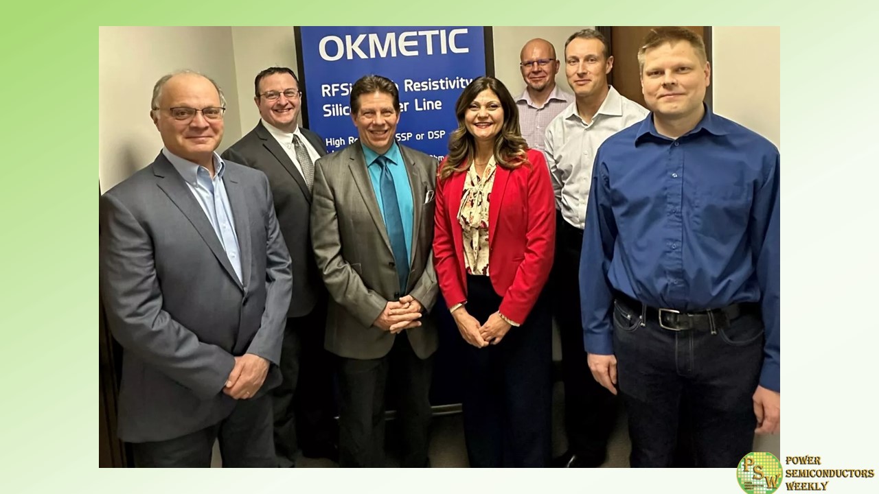
    Okmetic is celebrating the 25th anniversary of its North American sales office. Okmetic Inc. was established in Allen, Texas in 1999 to strengthen Okmetic sales and technical support to the North American customer base. The Okmetic, Inc. office continues to be based in Allen, Texas with local commercial support across North America.

    Initially, the business was focused on selected silicon products but has since expanded to support not only traditional semiconductor materials but also engineered products used for the Communication, RF filter, MEMS, Power, and AI just to highlight a few. The NA customer region, along with the European and Asian regions, work together using a balanced approach to serve the Okmetic worldwide market.

    The team at Okmetic Inc. continues to be recognized for support efforts in the industry.  Some of these include supplier award recognition, numerous conference speaking and exhibiting engagements, as well as a lifetime achievement recognition for company’s participation with organizations such as SEMI.

    “We want to thank our customers for entrusting us to be a key component of their business growth strategy, inspiring us to continuously raise the bar and cooperatively develop silicon products that enable our lives each day.  As we continue to expand our capacity to build for our future, we are excited to partner more closely with our customers to develop the needed products and support to enable their ongoing business needs “, says Jim Reed, President of Okmetic Inc.

    Original – Okmetic

    Comments Off on Okmetic Celebrates 25th Anniversary of its North American Sales Office in Texas
  • Okmetic Received Infineon Technologies’ Best Wafer Supplier Award

    Okmetic Received Infineon Technologies’ Best Wafer Supplier Award

    1 Min Read

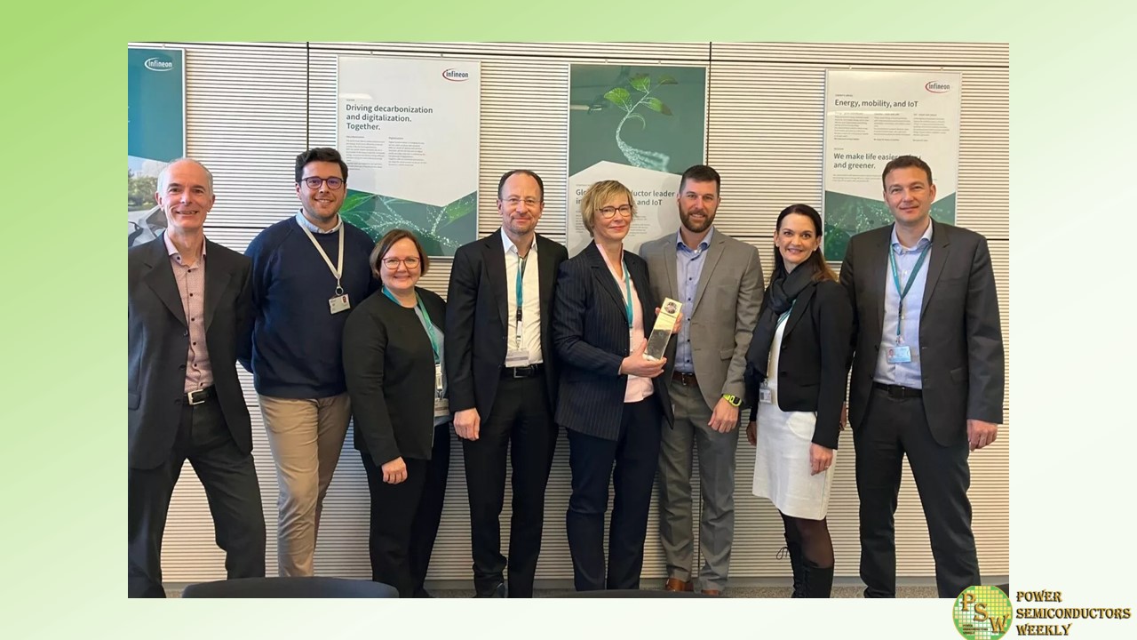
    Okmetic announced that the company has received Infineon Technologies’ Best Wafer Supplier award 2023. In their statement, Infineon Technologies described Okmetic as extremely supportive, agile and flexible, listening to the company needs.

    Okmetic expresses gratitude to Infineon for this recognition and for the continued trust and partnership.

    Infineon Technologies is a global semiconductor leader in power systems and IoT enabling game-changing solutions for green and efficient energy, clean and safe mobility, as well as smart and secure IoT. Okmetic is extremely proud to support Infineon Technologies with its silicon and SOI wafer solutions.

    Original – Okmetic

    Comments Off on Okmetic Received Infineon Technologies’ Best Wafer Supplier Award
  • Okmetic Expands Global Sales Network

    Okmetic Expands Global Sales Network

    1 Min Read

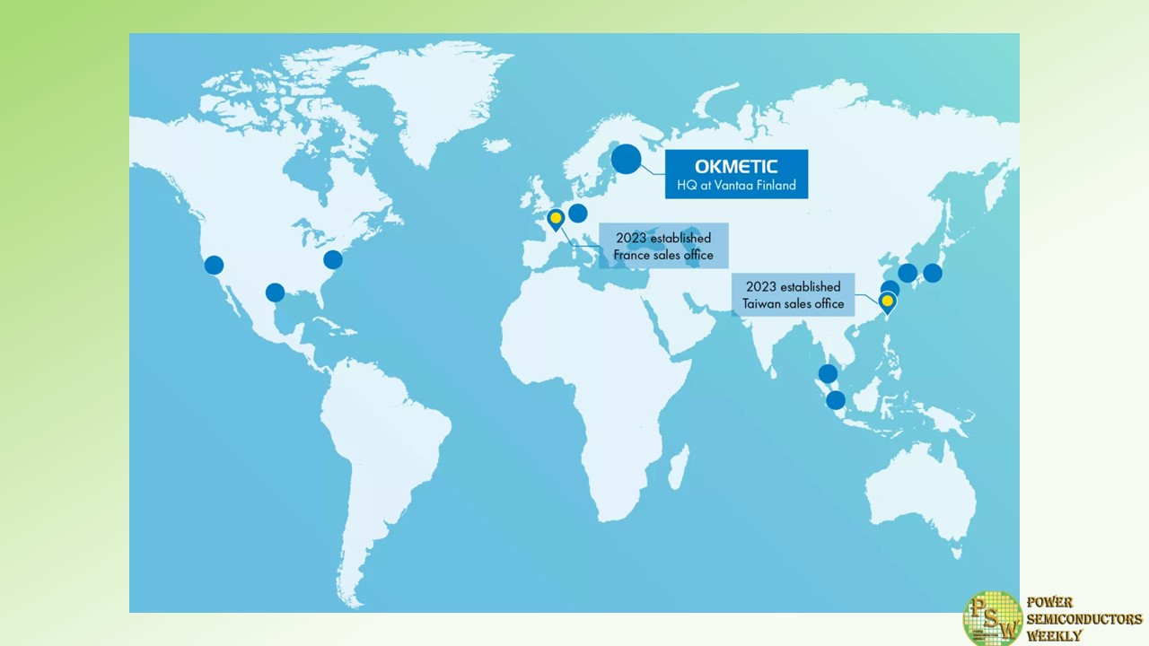
    Okmetic’s headquarters and production plant where most of silicon wafers are manufactured are located in Vantaa, Finland, while it is globally close to the customers. To better respond to local customers, the company is dedicated to improve its sales and customer support organization.

    During the year of 2023, Okmetic has established sales offices in both France and Taiwan to better serve the customers in these areas. This is one of commitments to take business operations to the next level.

    Since then on, company’s worldwide sales and service network is able to deliver quick expert responses from Finland, Germany, France, the United States, Japan, Taiwan and China. In addition, Okmetic’s network of agents is at full service in Korea, Malaysia and Singapore.

    Original – Okmetic

    Comments Off on Okmetic Expands Global Sales Network
  • Okmetic’s Senior Technology Development Manager Selected as Aalto University School of Electrical Engineering’s Alumnus of the Year 2023

    Okmetic’s Senior Technology Development Manager Selected as Aalto University School of Electrical Engineering’s Alumnus of the Year 2023

    3 Min Read

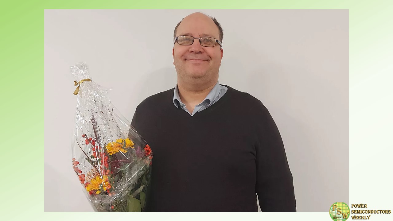
    Heikki Holmberg, Okmetic’s Senior Technology Development Manager, has been selected as Aalto University School of Electrical Engineering’s Alumnus of the Year 2023. Heikki graduated as a Master of Science (Technology) at the Electrical Department of the Helsinki University of Technology, the predecessor of Aalto University, in 2002. He defended his doctoral dissertation in 2008. The Alumnus of the Year award was presented to Heikki on Saturday 28.10.2023 at the Aalto Alumni Weekend seminar in Otaniemi. 

    Personnel, alumnus and students at Aalto University School of Electrical Engineering were able to propose the alumnus of the year during the spring and summer. The management team considered in their discussion Heikki’s great cooperation with the school and his role in bringing the semiconductor industry to the fore to be significant for the selection.

    “Heikki Holmberg knows the importance of cooperation between companies and the university, and he has coordinated the cooperation with our school in the Semi-Summer 2023 program and in highlighting the semiconductor industry in general. His work in his field is a great example for our students who are choosing their own study and career paths’, says Jussi Ryynänen, Dean of the Aalto University School of Electrical Engineering. 

    Heikki’s interest in the semiconductor industry was sparked already in the early days of his studies, and at the latest after the Basics of Semiconductor Industry course, it was clear that his future would lie in the field. Heikki describes the field as interesting, international and cross-disciplinary. The field combines materials physics, electro physics and chemistry. “The semiconductor industry is the industry of the future.” Heikki sums up. 

    Heikki has networked with other companies operating in the semiconductor industry in Finland and is an active member of several cooperation forums. “It is important that we cooperate with different companies in Finland to develop and advance the semiconductor industry. In this way, we will also be stronger at EU level.

    Okmetic has worked closely with Murata, Vaisala, Picosun and Kyocera for several years.” Heikki says. “Finland will need a significant number of new experts in the future, which is why cooperation with educational institutions is also important. The sector currently employs approximately 5,000 people in Finland, but the goal is to employ 20,000 people by 2032.” Heikki continues. 

    Heikki has also brought a lot of technological know-how and semiconductor industry experience to Okmetic. He himself says that his most significant achievements are projects related to the expansion of the patterning line and the development and launch of a new product (UF-RFSi™, Ultra Flat Radio Frequency Silicon Wafer), as well as the fact that most of the applications for EU support for various projects have received a positive decision.

    “Heikki’s expertise and energy have enabled Okmetic to react effectively to big opportunities and the challenges they contain. For this, a big thank you to Heikki and warm congratulations on a significant achievement on behalf of the entire Okmetic,” says Atte Haapalinna, CTO of Okmetic. 

    Original – Okmetic

    Comments Off on Okmetic’s Senior Technology Development Manager Selected as Aalto University School of Electrical Engineering’s Alumnus of the Year 2023
  • Okmetic Joins GaN Valley

    Okmetic Joins GaN Valley

    1 Min Read

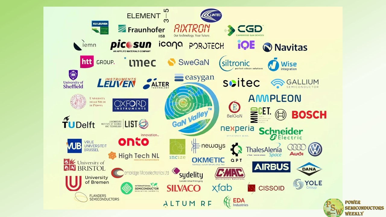
    GaN Valley™ is a connected ecosystem along the value chain of GaN technologies, products and electrical systems. It spans research and innovation (such as top-notch universities & RTOs), IDMs, Fabless Companies (including a growing industry of GaN start-ups & scale-ups), GaN Foundries, multi-market customers, as well as various Government Innovation instances. 

    Okmetic is now a part of GaN Valley™ community and looks forward to cooperation with other members in the GaN ecosystem! 

    Okmetic supplies substrate wafers for both RF and Power GaN devices. Its silicon substrate wafers are designed to endure the demanding GaN epitaxial process conditions and provide reduced wafer bow and warpage.

    Original – Okmetic

    Comments Off on Okmetic Joins GaN Valley
  • Okmetic Presented Customized Silicon and SOI Wafers at the ISES EU Power Event in Italy

    Okmetic Presented Customized Silicon and SOI Wafers at the ISES EU Power Event in Italy

    1 Min Read

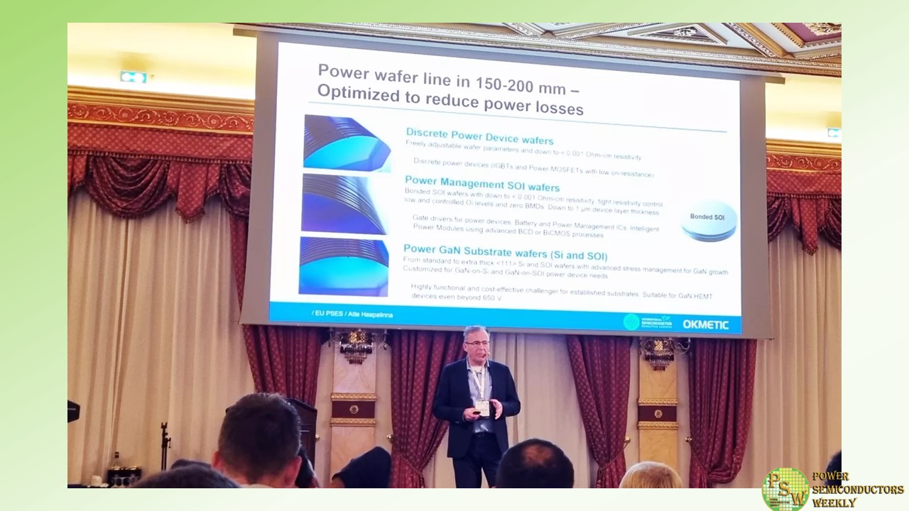
    Okmetic CTO Atte Haapalinna gave a speech in September 2023 at the ISES EU Power event on Customized Silicon and SOI Wafers Enabling Enhanced Power Devices.

    Advanced silicon wafers can greatly improve power device performance and reduce power losses. Okmetic Power wafer line provides an optimal platform for the manufacture of various power devices. Power device optimized wafer solutions improve power device performance, reduce Total Cost of Ownership and enable more refined designs.

    Okmetic Power wafer line comprise:

    Read more about Okmetic’s Power wafer line: Power Wafer Line | Okmetic

    Original – Okmetic

    Comments Off on Okmetic Presented Customized Silicon and SOI Wafers at the ISES EU Power Event in Italy