-

The accelerated transition to electric vehicles has led to significant innovations in charging systems that demand more cost-efficient and high performing power electronics. Addressing this, Infineon Technologies AG expands its 650 V CoolMOS™ CFD7A portfolio by introducing the QDPAK package.
This package family is designed to provide equivalent thermal capabilities with improved electrical performance over the well-known TO247 THD devices, thus enabling efficient energy utilization in onboard chargers and DC-DC converters.
Efficient and powerful electric vehicle charging systems help reduce charging times and vehicle weight, increasing design flexibility and reduce the total cost of ownership of the vehicle. This new addition complements the existing CoolMOS CFD7A series, offering versatility with top-side and bottom-side cooled packages. The QDPAK TSC (top side cooled), enables designers to achieve higher power densities and optimal PCB space utilization.
The 650 V CoolMOS CFD7A offers several important features for reliable operation in high-voltage applications. Thanks to its reduced parasitic source inductance, the device can minimize electromagnetic interference (EMI), ensuring clear signals and consistent performance.
The Kelvin source pin also provides improved precision for current sensing, ensuring accurate measurements even in challenging conditions. With a creepage distance suitable for high voltage applications, as well as high current capability and high power dissipation (P tot) of up to 694 W at 25°C, it is a versatile and powerful device for a wide range of high-voltage applications.
New system designs using 650 V CoolMOS CFD7A in QDPAK TSC will maximize PCB space use, doubling power density and enhancing thermal management via substrate thermal decoupling. This approach simplifies assembly, eliminates board stacking and reduces the need for connectors, thereby lowering system costs. The power switch reduces thermal resistance by up to 35 percent, providing high power dissipation that outperforms standard cooling solutions.
This feature overcomes the thermal limitations of bottom side cooled SMD designs using FR4 PCBs, resulting in a significant boost in system performance. The optimized power loop design locates drivers near the power switch, improving reliability by reducing stray inductance and chip temperatures. Overall, these features contribute to a cost-effective, robust, and efficient system ideal for modern power needs.
As announced in February 2023, the QDPAK TSC package has been registered as a JEDEC standard for high-power applications, helping to establish a broad adoption of TSC in new designs with one standard package design and footprint. To further to accelerate this transition, Infineon will also release additional Automotive Qualified devices in QDPAK TSC for onboard chargers and DC-DC converters in 2024, such as 750 V and 1200 V CoolSiC™ devices.
Original – Infineon Technologies
-
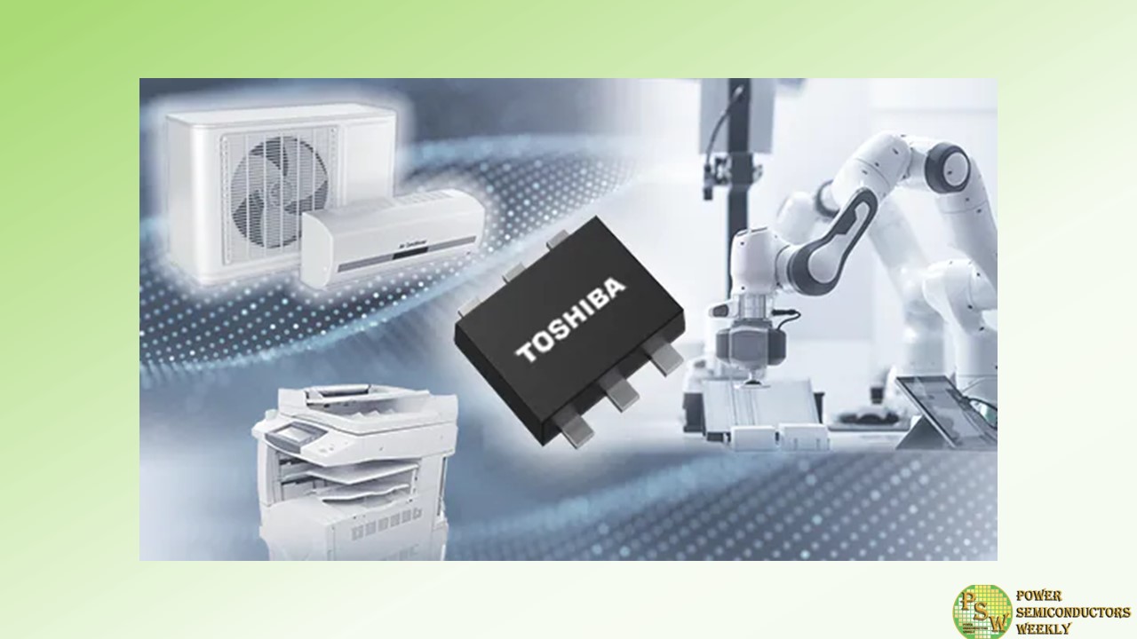
Toshiba Electronic Devices & Storage Corporation has launched the product “HN1D05FE”, a 400 V voltage switching diode. The new product “HN1D05FE” is suitable for applications that require high voltage characteristics such as commercial AC power supply circuits and AC-DC converter circuits for LED illumination. With a 400 V reverse voltage rating, HN1D05FE is suitable for power supply circuits below 200 V, as well as reverse-current protection and surge protection, and more.
In addition, the new product is housed in a SOT-563 package (Toshiba package name: ES6, 1.6 mm × 1.6 mm (typ.), t=0.55 mm (typ.)) to achieve high voltage characteristics in a small size.
Furthermore, built-in two switching diodes allow reducing the number of devices in circuits which use multiple devices.Moreover, the package size is reduced by approximately 70 % and the package height is as low as 50 % compared with the SOT-24 package (Toshiba package name: SMQ, 2.9 mm × 2.9 mm (typ.), t=1.1 mm (typ.)) of Toshiba’s existing product 1SS399. This helps to downsizing and thinning of the set.
Applications
- Consumer equipment (home appliances, OA equipment, PC, etc.)
- Industrial equipment (FA equipment, PV, semiconductor-manufacturing equipment, etc.)
Features
- High reverse voltage : VR = 400 V
- Low leakage current : IR = 0.1 μA (max) (VR = 400 V)
- Small and thin SOT-563 Package : Toshiba Package Name : ES6 (1.6 mm × 1.6 mm (typ.), t = 0.55 mm (typ.))
Original – Toshiba
-
Resonac Corporation will take part in a consortium of semiconductor-related manufacturers named “Texas Institute for Electronics”, which is located in the state of Texas, USA. Resonac will be the first Japanese member of TIE as a semiconductor material manufacturer.
TIE is a non-profit organization led by The University of Texas at Austin, and consists of the public and private sectors including the state of Texas, semiconductor manufacturers, defense electronics manufacturers, national laboratories, and academic bodies.
Its aim is to advance the roadmap of cutting-edge semiconductor systems by five years (or more than two generations), and to develop them in the United States.. TIE’s strategic member companies include leading semiconductor manufacturers such as AMD, Inc., Micron Technology, Inc., Intel Corporation, Applied Materials, Inc., etc.
Resonac was invited to participate as the strategic member from the materials manufacturers, as it was recognized by TIE for the comprehensive lineup of materials for the front-end and back-end processes used in advanced semiconductors, R&D organization specializing in semiconductor packaging “Packaging Solution Center,” and track record in operating the consortium “JOINT2” composed of semiconductor-related companies. TIE plans to launch a prototype line for wafer-scale 2xD and 3D advanced packaging starting from the second half of 2024.
Semiconductors support the lives of the people as social infrastructure. Development of leading-edge semiconductors to be used for AI and next-generation telecommunication requires cooperation between manufacturers of devices, materials, and equipment. Resonac will aim to cooperate with other companies through its participation in TIE, research and development of leading-edge technologies and contributions to solutions of problems concerning semiconductors.
Aiming to accomplish its purpose, “Change society through the power of chemistry,” Resonac will strive to promote co-creation, and contribute to improvement in semiconductors’ performance, which is needed by society.
Original – Resonac
