-
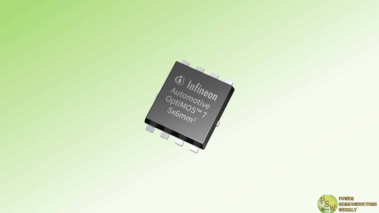
Infineon Technologies AG introduced the first product in its new advanced power MOSFET technology OptiMOS™ 7 80 V. The IAUCN08S7N013 features a significantly increased power density and is available in the versatile, robust, and high-current SSO8 5 x 6 mm² SMD package.
The OptiMOS™ 7 80 V offering is a perfect match for the upcoming 48 V board net applications. It is designed specifically for the high performance, high quality and robustness needed for demanding automotive applications like automotive DC-DC converters in EVs, 48 V motor control, for instance electric power steering (EPS), 48 V battery switches and electric two- and three-wheelers.
Compared to the previous generation, the R DS(on) of the Infineon IAUCN08S7N013 has been reduced by more than 50 percent, and is now the best R DS(on) in the industry with a maximum of 1.3 mΩ. Users benefit from minimized conduction losses, superior switching performance and the highest power density in a 5 x 6 mm² package.
In addition, the IAUCN08S7N013 also features low package resistance and inductance, as well as a high avalanche current capability. For automotive applications, it has an extended qualification that goes beyond AEC-Q101.
The IAUCN08S7N013 is in mass-production and available now. More information is available at www.infineon.com/iaucn08s7n013/.
Original – Infineon Technologies
-
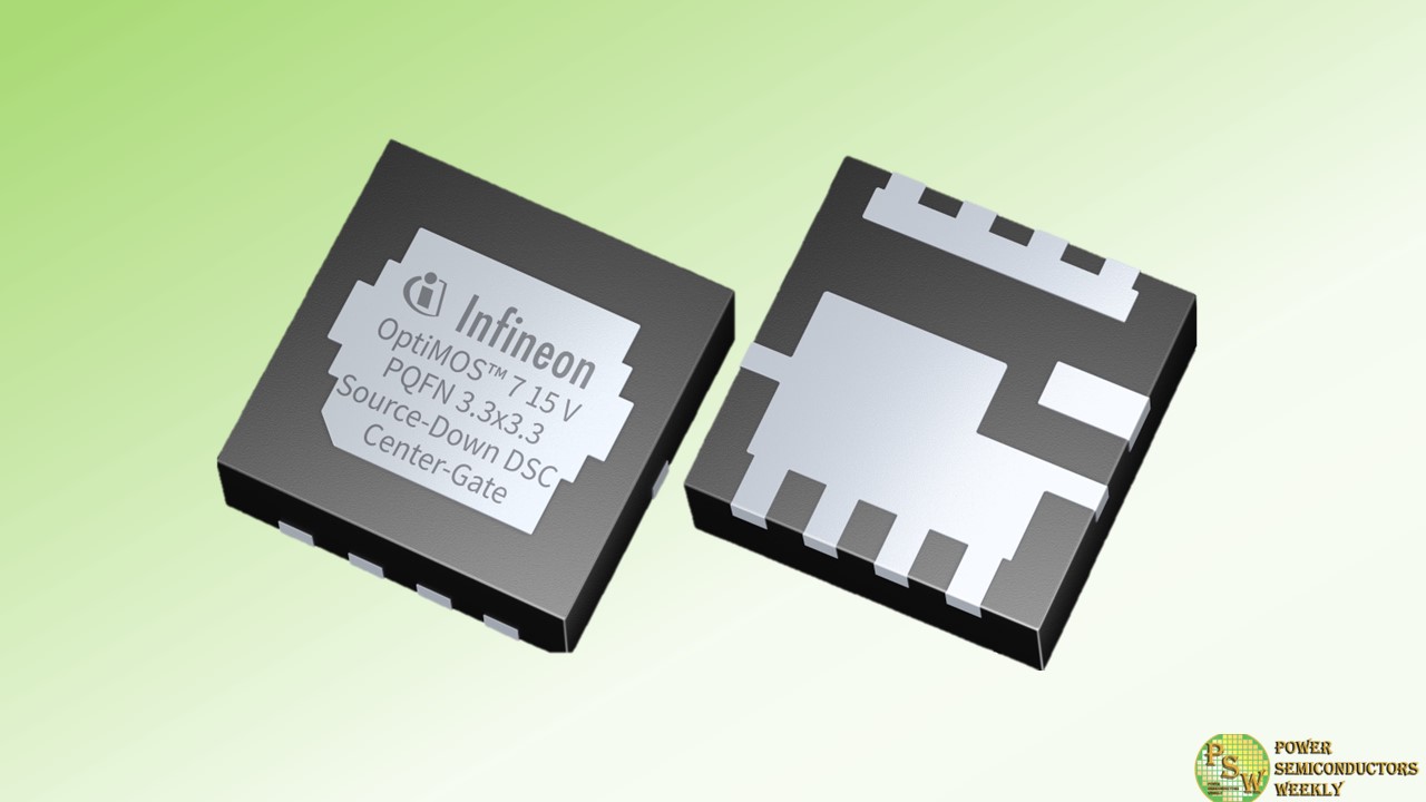
The ever-increasing power demand in data centers and computing applications requires advancements in power efficiency and compact power supply design. Infineon Technologies AG responds to trends on the system level by introducing its new OptiMOS™ 7 family, industry’s first 15 V trench power MOSFET technology. The OptiMOS 7 15 V series primarily targets optimized DC-DC conversion for servers, computing, datacenter, and artificial intelligence applications.
The product portfolio includes the latest PQFN 3.3 x 3.3 mm² Source-Down, with bottom- and dual-side cooling variants in standard- and center-gate footprints. The portfolio also includes a robust PQFN 2 x 2 mm² variant with a reinforced clip. The OptiMOS 7 15 V technology is specifically tailored for DC-DC conversions with low output voltages, particularly in server and computing environments. This advancement aligns with emerging shifts towards high ratio DC-DC conversion in data-center power distribution.
Compared to the established OptiMOS5 25 V, the new OptiMOS 7 15 V achieves a reduction of R DS(on) and FOMQ g by ~30 percent, and FOMQ OSS by ~50 percent by lowering the breakdown voltage. The PQFN 3.3 x 3.3 mm² Source-Down package variants provide a more versatile and effective PCB-design. Furthermore, the PQFN 2 x 2 mm² package provides a pulsed current capability higher than 500 A and a typical R thJC of 1.6 K/W.
By minimizing conduction and switching losses and incorporating advanced packaging technology, thermal management becomes easy and effective, setting new benchmarks both for power density and overall efficiency.
Original – Infineon Technologies
