-
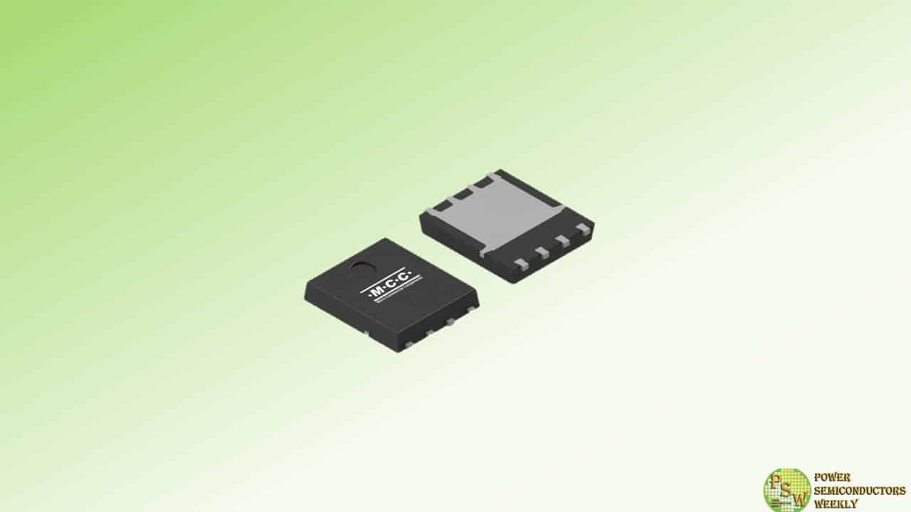
Micro Commercial Components introduced the latest auto-grade N-channel power MOSFETs with up to 2.5mΩ on-resistance: MCACL220N06YHE3, MCACL2D5N06YL, MCACL280N04YHE3, and MCACL330N04YHE3.
Optimized for high current output, these powerful components boast RDS(on) as low as 0.8mΩ in a sleek, engineer-friendly DFN5060 package. You can enhance power management and ramp up efficiency with minimal losses and the confidence that come along with AEC-Q101 qualification and the MCC name.
With high power density, MCC’s new 40V and 60V MOSFETs are designed to handle harsh conditions and operating junction temps up to 175℃ with ease, making them ideal for diverse automotive and industrial applications — from battery management systems and electric power steering to lighting controls, water pumps, and solar power systems.
Features & Benefits:
- AEC-Q101 qualified for reliability
- Advanced split-gate trench (SGT) technology
- Excellent thermal performance & efficiency
- Low RDS(on) minimizes power losses
- High power density packagey
- High junction temperature up to 175℃
- Compact DFN5060 package saves space and material costs
Original – Micro Commercial Components
-
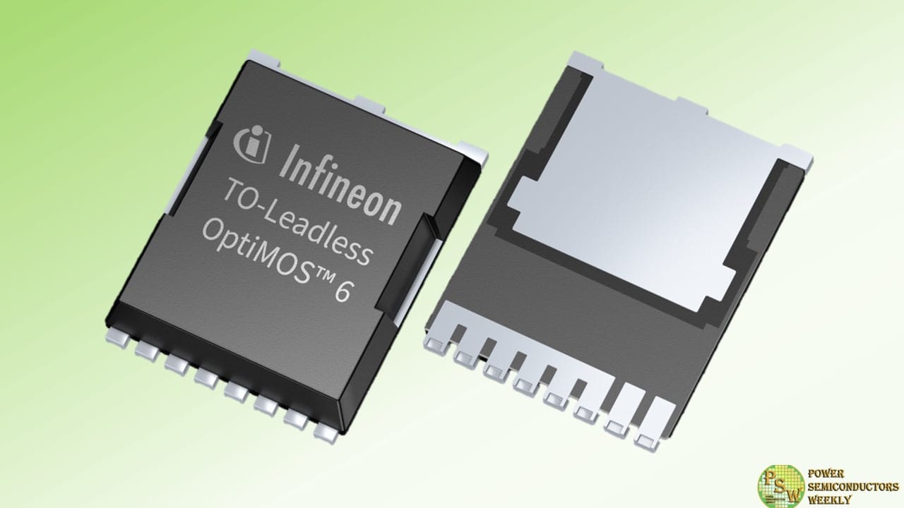
Motor drive applications are taking a leap forward with the launch of the Infineon Technologies AG OptiMOS™ 6 200 V MOSFET product family. The new portfolio is designed to deliver optimal performance in applications such as e-scooters, micro-EVs, and E-forklifts.
The improved conduction losses and switching behavior for these new MOSFETs reduce the electromagnetic interference (EMI) and switching losses. This benefits various switching applications, including servers, telecom, energy storage systems (ESS), audio, solar and others.
Additionally, the combination of a wide safe operating area (SOA) and industry-leading R DS(on) results in a perfect fit for static switching applications such as battery management systems. With the introduction of the new OptiMOS 6 200 V product family, Infineon sets a new industry benchmark with increased power density, efficiency, and system reliability for its customers’ benefit.
The OptiMOS 6 200 V portfolio delivers enhanced technical features compared to its predecessor, the OptiMOS 3. It features a 42 percent lower R DS(on) that contributes to reduced conduction losses and increased output power. Regarding diode behavior, the OptiMOS 6 200 V provides a significant increase in softness, more than three times that of the OptiMOS 3.
Combined with up to 89 percent reduction in Q rr(typ), the switching and EMI behaviors are significantly improved. The technology also features improvements in parasitic capacitance linearity (C oss and C rss), which reduces oscillation during switching and lowers voltage overshoot. A tighter V GS(th) spread and lower transconductance aid in MOSFET paralleling and current sharing, leading to more uniform temperatures and reducing the number of paralleled MOSFETs.
The OptiMOS 6 200 V products feature an improved SOA and are classified as MSL 1 according to J-STD-020. These RoHS-compliant, lead-free products align with current industry standards.
Original – Infineon Technologies
-
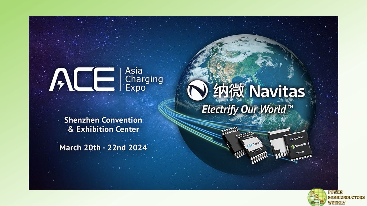
Navitas Semiconductor announced its participation in the forthcoming 2024 Asia Charging Expo (ACE) in Shenzhen, China, from March 20th to 22nd, 2024. Visitors will explore the latest advances in GaN and SiC toward a fully-electrified “Planet Navitas” and the transition from fossil fuels.
Navitas will introduce the latest GaNFast™ and GeneSiC™ products to the audience in China for the first time, including: GaNSense™ half-bridge power ICs with application-specific features and higher power ratings, Gen-3 Fast SiC power FETs for high-power and higher-speed performance, and the world’s most protected GaN power devices – GaNSafe™.
Teaming up with UGREEN, Navitas will showcase a variety of UGREEN fast chargers featuring GaNFast power ICs, including the adorable and popular 30W and 65W Nexode Robot chargers, 100W Nexode Magsafe Charger Stand, and high-power 300W Nexode 5-port Desktop Charging Station. Many more GaNFast™ chargers will be displayed for visitors to experience the lightning speed of GaNFast charging.
Ye Hu, Navitas’ Technical Marketing Manager, will deliver a keynote presentation titled “A New Chapter in GaN: Navitas’ Integrated Drive and Loss-less Current Sensing GaNSense™ Half-bridge Solution” as part of the exposition’s World GaN Conference on March 22nd.
ACE 2024 will be held at Hall 6, Futian Convention and Exhibition Center, Shenzhen, China from March 20th to 22nd. Visitors to “Planet Navitas” (booth B57-B60) will meet experienced Navitas engineers to explore the power of next-gen power semiconductors for leading-edge applications. Navitas sales and distribution partners will also provide on-site support.
“The Asia Charging Expo is a critical event in the power electronics industry – gathering key experts from mobile, EV and industrial companies – and we are delighted to be part of it again to present our latest GaN and SiC technology,” said Charles Zha, VP and GM of Navitas China. “Our latest, advanced GaNFast and GeneSiC technologies bring revolutionary fast-charging capabilities to industry-leading Chinese customers.”
Original – Navitas Semiconductor
