-
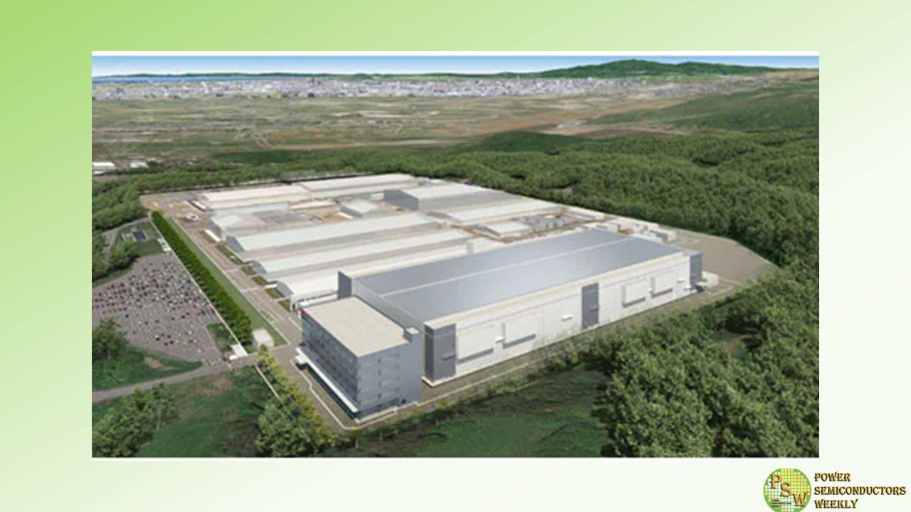
Toshiba Electronic Devices & Storage Corporation (“Toshiba”) announced that it has started construction of a new wafer fabrication factory for power semiconductors at Kaga Toshiba Electronics Corporation, in Ishikawa Prefecture, Japan, its main discrete semiconductor production base. Construction will take place in two phases, with the production start of Phase 1 scheduled for within fiscal 2024. Toshiba will also construct an office building adjacent to the new fab to respond to the increase in personnel.
The new fab will have a quake absorbing structure and enhanced BCP systems, including dual power supply lines, and also aim to use 100% renewable energy. Product quality and production efficiency will be improved by introducing artificial intelligence systems and other measures.
Toshiba started power semiconductor production on a 300-milimeter wafer line in the second half of fiscal 2022. Going forward, Toshiba will expand production capacity of power semiconductors with the new fab and further contribute to carbon neutrality.
Original – Toshiba
