-
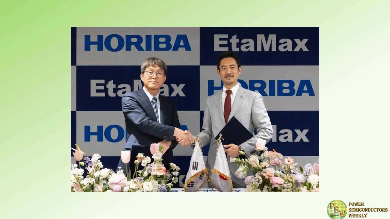
HORIBA STEC KOREA, Ltd., a HORIBA subsidiary responsible for the Group’s semiconductor business in South Korea, has acquired EtaMax Co., Ltd., a developer, manufacturer, and seller of wafer inspection system for the semiconductor market. The share transfer was completed on April 3, 2025.
The HORIBA Group aims to expand its lineup of wafer inspection system and enhance its solution-proposal capabilities by integrating spectroscopy-related technologies developed in-house over many years with EtaMax’s software technology and extensive expertise in inspecting for defects in compound semiconductor wafers. This integration will contribute to boosting yield and enhancing quality control for compound semiconductor wafers.
The increasing demand for data centers driven by the global expansion of EVs and AI is accelerating the adoption of compound semiconductors, known as next-generation power semiconductors. While compound semiconductors offer high performance and durability, loss of yield in the manufacturing process due to wafer defects remains a challenge, creating a strong demand for precise and efficient inspections.
The HORIBA Group aims to achieve sales of 235 billion yen by 2028 in the Materials & Semiconductor field—a key area of focus in the Group’s Mid-Long Term Management Plan (MLMAP2028). In pursuing such vision for this field—to shape the market with innovative solutions in the advanced materials and semiconductor field toward achieving sustainable society—it was essential to bolster R&D of compound semiconductor wafer inspection system in order to provide comprehensive analytical solutions that enhance the semiconductor manufacturing process.
EtaMax primarily develops wafer inspection system utilizing photoluminescence analysis technology. The company excels in a diverse range of applications, including assessing uniformity and identifying types of minute defects in compound semiconductor wafers.
This acquisition will allow to leverage the HORIBA Group’s extensive global network to drive business expansion. Furthermore, we the company will be able to accelerate new product development and enhance the solution-proposal capabilities by synergizing EtaMax’s software technologies with the HORIBA Group’s core technologies, such as Raman spectroscopy and ellipsometry. This will aid in boosting yield and enhancing quality control in the process of mass-producing compound semiconductor wafers.
The HORIBA Group is committed to creating new value to meet the diverse analysis and measurement needs of the customers in the semiconductor manufacturing process.
Original – HORIBA STEC KOREA
